Semiconductor component and sensor component for data transmission devices

a technology of data transmission device and semiconductor, applied in the direction of semiconductor device, semiconductor/solid-state device details, electrical apparatus, etc., can solve the problem of limited energy transmission, and achieve the effect of avoiding electrical connections and increasing the throughput of biochemical samples

Inactive Publication Date: 2005-05-19
INFINEON TECH AG
View PDF6 Cites 11 Cited by
  • Summary
  • Abstract
  • Description
  • Claims
  • Application Information

AI Technical Summary

Benefits of technology

[0030] This method has the advantage that a respective sensor component can be used for different biochemical samples, which sensor component is subsequently destroyed as a disposal product. For this purpose, as mentioned above, the sensor component has merely three components, namely a sensor chip, a coupling element coupled thereto for wireless transmission, and a housing composition that partly embeds the sensor chip and completely embeds the coupling element. Further, the method has the advantage that the placement of the sensor component with a sample onto the semiconductor component can be effected relatively non-critically, since the coupling elements do not have to be exactly opposite one another for the wireless transmission. Rather, it suffices for the sensor component with its coupling element to be brought into the local region of the coupling element of the semiconductor component in order to ensure both the energy transmission and the signal transmission.
[0031] An implementation of the method may furthermore have the following steps. Firstly, the semiconductor component calls up sensor data from the sensor component via its main coupling element, whereupon the sensor component supplies, via the sensor coupling element, sensor results to the semiconductor component via the main coupling element thereof for evaluation and storage. This method has the advantage that the mode of operation of sensor component and semiconductor component depends only on the coupling effect of the two coupling elements. An optical transmission is not provided in this implementation of the method.
[0032] A further implementation of the method provides for the semiconductor component to call up sensor data via the main coupling element and for the sensor component thereupon to supply sensor results optically to the semiconductor component for evaluation and storage. In this exemplary implementation of the method, a transmission of the signals is carried out only in one direction, namely from the semiconductor component via the main coupling element to the sensor coupling element, but not in the opposite direction from the sensor coupling element to the main coupling element. Rather, the second possibility of the sensor stack, in the case of which the optical transmission path is used, is utilized. This optical transmission path from the sensor component to the semiconductor component has the advantage that the optical transmission path is insensitive to electromagnetic interference fields.
[0033] Furthermore, provision is made for arranging and testing a plurality of biochemical samples simultaneously on a semiconductor component. Given a design with a sufficiently large area, a plurality of sensor components with smaller coupling elements than the main coupling element may be arranged in the region of the coupling element of the semiconductor component. This has the advantage that mass examinations become possible in a cost-effective manner.
[0034] Furthermore, the method according to the invention provides for measurement results and / or evaluation results to be forwarded from the integrated circuit of the semiconductor component to a superordinate circuit via external contacts of the semiconductor component. This concept makes it possible for a plurality of semiconductor components to be arranged on the superordinate circuit board, so that the throughput of measurements of biochemical samples can be increased further. It is possible to populate entire trays with semiconductor components, with the semiconductor components having a plurality of sensor components stacked thereon one next to the other.
[0035] The invention affords the possibility of multiple sensor applications without direct electrical contact between sensor component and semiconductor component, which may have a logic chip. A further advantage is the single application in multiple biological tests by means of the semiconductor sensors. Finally, the invention provides the advantage of avoiding electrical connections for the sensor stack, so that, merely after each sample detection and sample measurement, only the sensor component has to be discarded after simply being removed, pushed down or sucked away from the semiconductor component.

Problems solved by technology

Even a limited energy transmission is possible via the main coupling element.

Method used


Image

  • Semiconductor component and sensor component for data transmission devices
  • Semiconductor component and sensor component for data transmission devices
  • Semiconductor component and sensor component for data transmission devices

Examples


Embodiment Construction

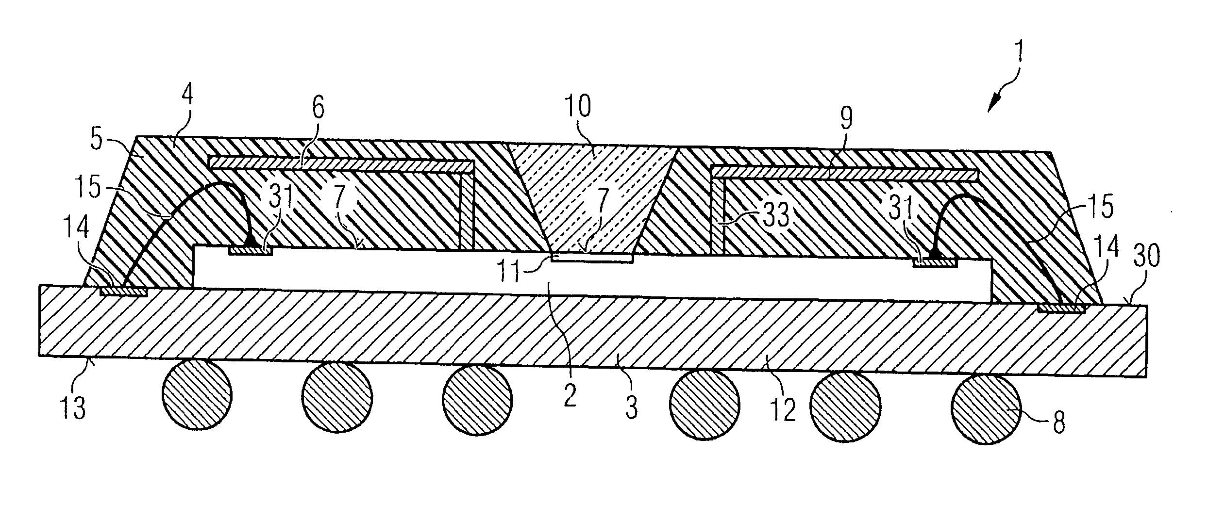
[0046]FIG. 1 shows a diagrammatic cross section through a semiconductor component 1 with a semiconductor chip 2, in accordance with an embodiment of the present invention. The semiconductor component 1 has a substrate 3 with a rewiring structure. On its underside 13, the substrate 3 has external contacts 8, which are connected via through contacts through the substrate 3 to rewiring lines on a top side 30 of the rewiring substrate 12. The rewiring lines (not shown in FIG. 1) lead to bonding contact pads 14 that are arranged on the top side of the rewiring substrate 12.

[0047] By virtue of this arrangement of external contacts 8 with through contacts and rewiring lines, and also with bonding contact pads 14, the entire underside 13 of the rewiring substrate 12 can be utilized for the fitting of external contacts 8, even though the semiconductor chip 2 is arranged on the top side 30 of the rewiring substrate 12. The semiconductor chip 2 carries an integrated circuit with logic functio...


PUM


Abstract

The invention relates to a semiconductor component and a sensor component with data transmission devices, for wireless transmission the semiconductor component having a main coupling element and the sensor component having a sensor coupling element. The invention affords the possibility of multiple sensor applications without direct electrical contact between sensor component and semiconductor component, which may have a logic chip.

Description

CROSS REFERENCE TO RELATED APPLICATIONS [0001] This application claims priority under 35 USC § 119 to German Application No. DE 103 46 474.3, filed on Oct. 2, 2003, and titled “Semiconductor Component and Sensor Component for Data Transmission Devices,” the entire contents of which are hereby incorporated by reference. BACKGROUND OF THE INVENTION [0002] 1. Field of the Invention [0003] The present invention relates generally to components for wireless, data transmission devices and, more particularly to a semiconductor component employing a main coupling element and a sensor component employing a sensor coupling element. [0004] 2. Description of the Related Art [0005] Systems such as transponder units and smart card systems typically include at least two components: a station and a response circuit, which interact wirelessly to form a data transmission circuit. The station employs a primary coil and a signal generator for generating an alternating magnetic field with a carrier frequ...

Claims


Application Information

Patent Timeline
Patent Type & Authority Applications(United States)
IPC IPC(8): H01L23/31H01L23/48H01L23/498H01L23/66H01L25/10H01L31/0203
CPCH01L23/3128H01L23/48H01L2924/01021H01L24/48H01L2924/3011H01L2924/19041H01L2924/1815H01L2924/15311H01L2224/48465H01L2224/48227H01L2224/48091H01L23/49855H01L23/66H01L25/105H01L31/0203H01L2223/6677H01L2924/00014H01L2924/00H01L2924/12043H01L2924/14
Inventor BAUER, MICHAELENGLING, THOMASHAIMERL, ALFREDMAHLER, JOACHIMSCHOBER, WOLFGANG
Owner INFINEON TECH AG
Why Eureka
Try Eureka