

Two-Dimensional Photonic Crystal MicroArray Measurement Method and Apparatus for Highly-Sensitive Label-Free Multiple Analyte Sensing, Biosensing, and Diagnostic Assay
a photonic crystal and microarray technology, applied in the field of optical and medical devices, can solve the problems of poor quality, inconvenient design for the fabrication of microarrays for multiple analyte sensing, and use of microcavities, and achieve the effects of improving sensitivity, reducing refractive index, and increasing the measurement throughput of the devi
- Summary
- Abstract
- Description
- Claims
- Application Information
AI Technical Summary
Benefits of technology
Problems solved by technology
Method used
Image

Examples
Embodiment Construction
Detailed Description of the Invention
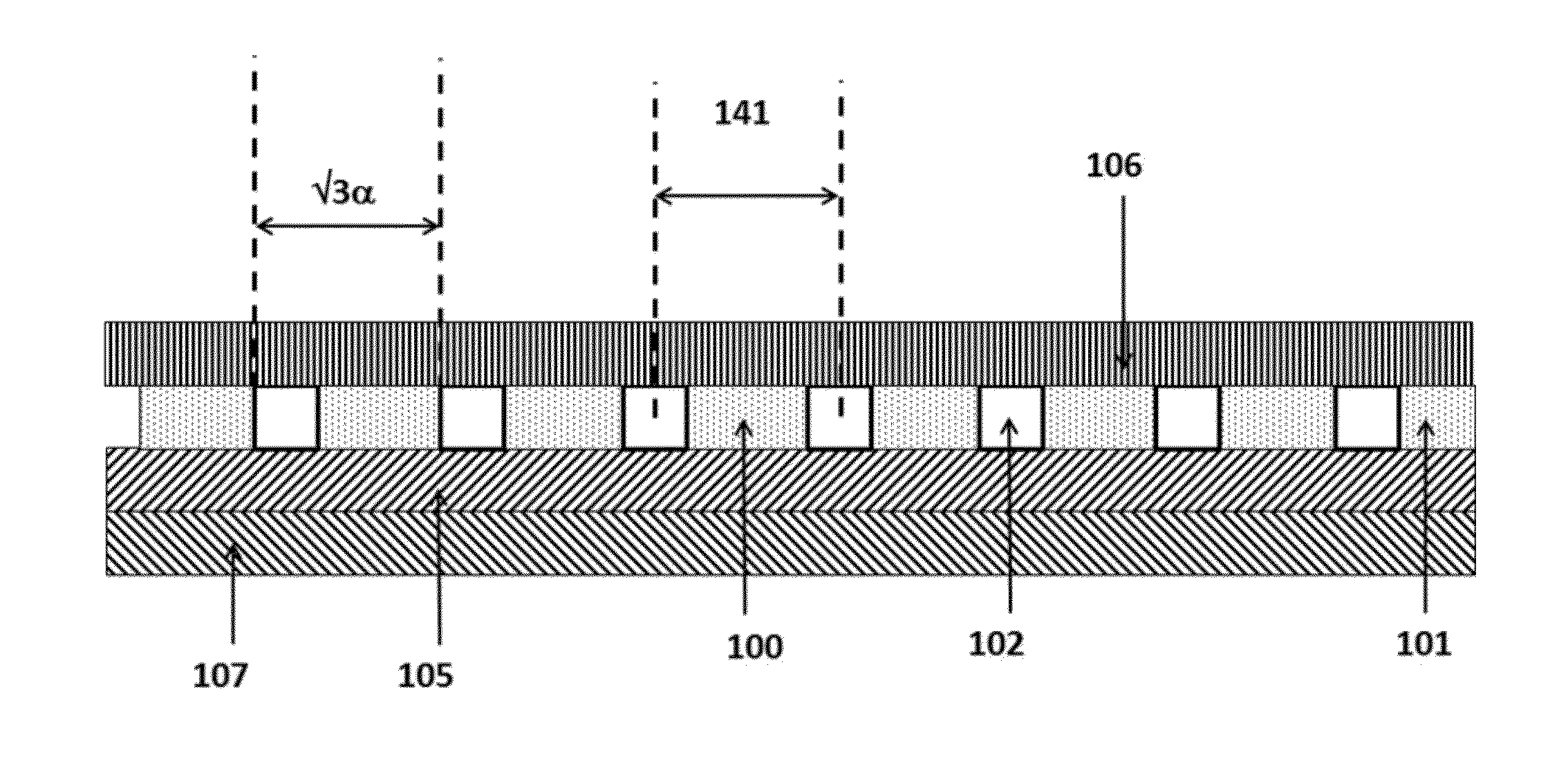
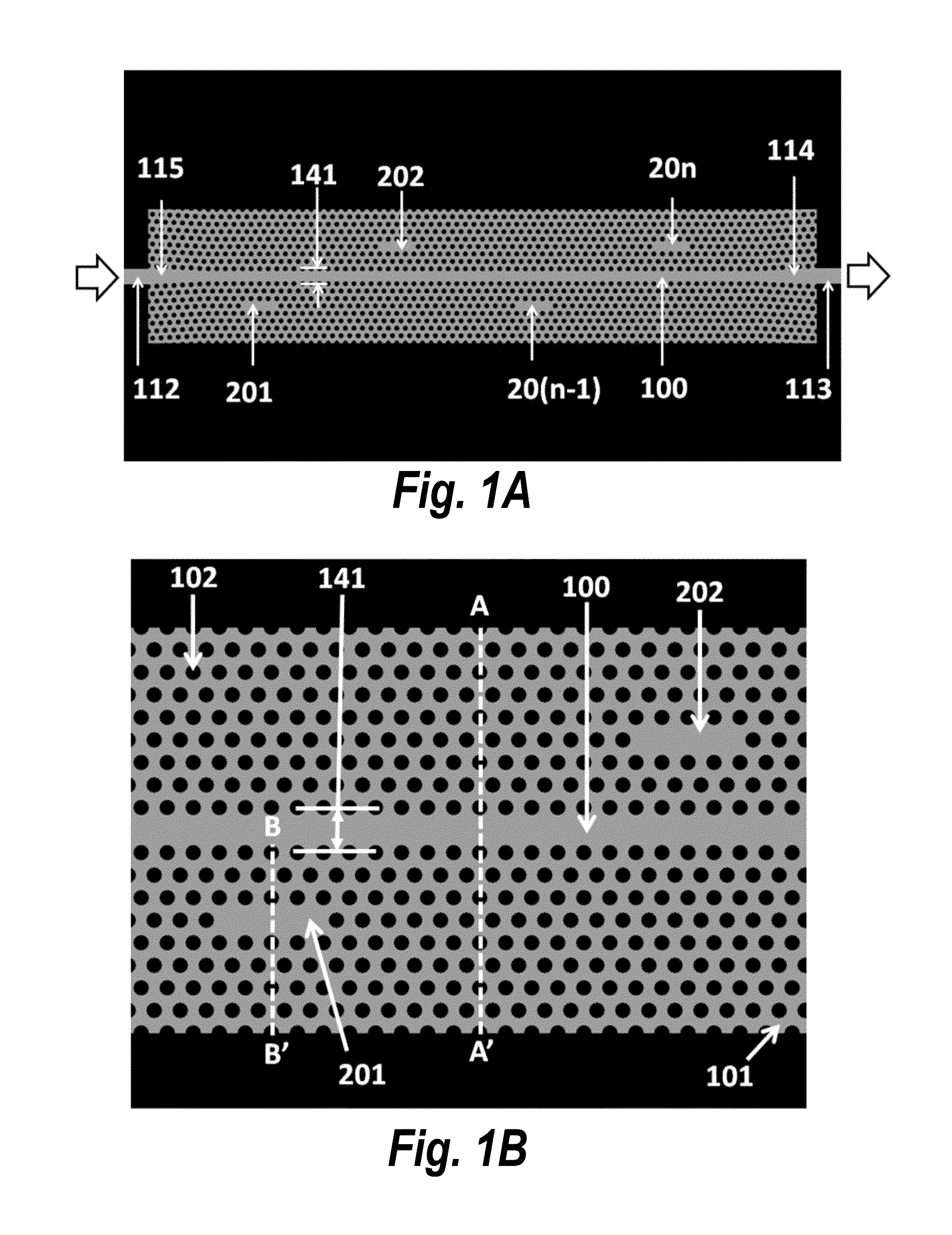
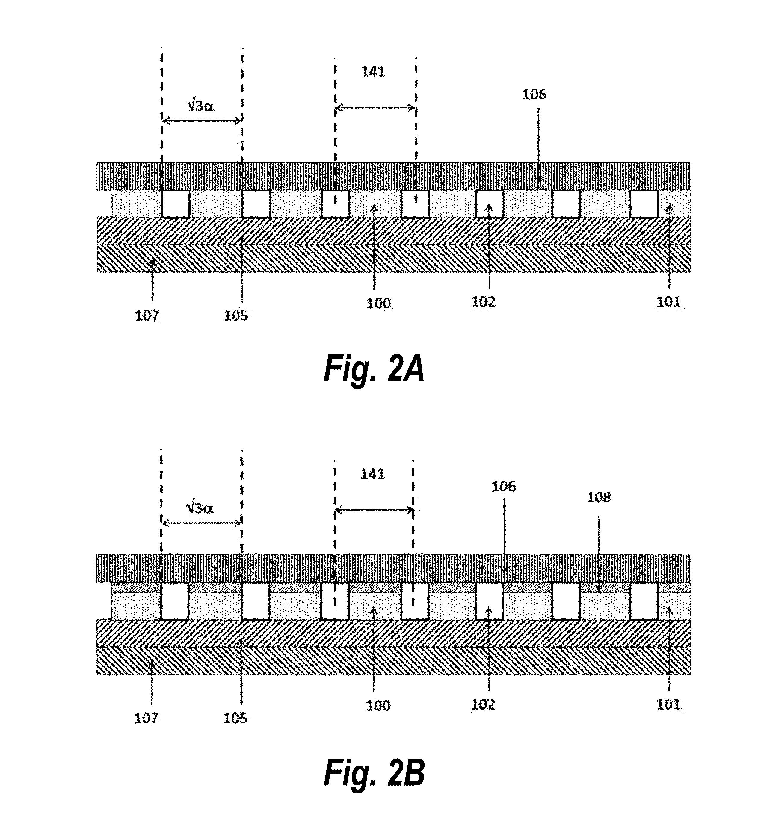
[0041]In accordance with a preferred embodiment of the present invention, a device for a microarray for personalized diagnostic applications comprises: a functional photonic crystal waveguide having a waveguide core along which light is guided, arrays of photonic crystal microcavities along the length of the photonic crystal waveguide each coated with a separate target binding molecule specific to disease identification, an input and output photonic crystal waveguide with gradually changed group index before and after the functional photonic crystal waveguide, which can bridge the refractive indices difference between conventional optical waveguides and the functional photonic crystal waveguide. The sensor can be used to detect organic or inorganic substances such as proteins, DNA, RNA, small molecules, nucleic acids, virus, bacteria, cells, and genes, without requiring labels such as fluorescence or radiometry. Light (from a broadband source or ...
PUM
| Property | Measurement | Unit |
|---|---|---|
| temperature | aaaaa | aaaaa |
| temperature | aaaaa | aaaaa |
| thickness | aaaaa | aaaaa |
Abstract
Description
Claims
Application Information