Semiconductor device

a technology of semiconductors and devices, applied in the direction of semiconductor devices, electrical equipment, transistors, etc., can solve the problems of affecting the operation of semiconductor devices, so as to facilitate the improvement of reverse withstand voltage, facilitate the improvement, and facilitate the preventing the waveform of turnoff voltage and the waveform of turnoff current from oscillating

Active Publication Date: 2011-06-30
FUJI ELECTRIC CO LTD
View PDF2 Cites 7 Cited by
  • Summary
  • Abstract
  • Description
  • Claims
  • Application Information

AI Technical Summary

Benefits of technology

The semiconductor device according to the invention facilitates improving the reverse withstand voltage thereof. The semiconductor device according to the invention facilitates improving also the forward withstand voltage thereof. The semiconductor device according to the invention facilitates preventing the turnoff voltage waveform and the turnoff current waveform from oscillating. The semiconductor device according to the invention facilitates suppressing the oscillations caused on the reverse recovery voltage waveform and the reverse recovery current waveform.

Problems solved by technology

In the case, in which the turnoff waveforms and the reverse recovery waveforms oscillate, the semiconductor device may be broken down, when noises are caused or when very large oscillations are caused on the voltage waveform.

Method used


Image

  • Semiconductor device
  • Semiconductor device
  • Semiconductor device

Examples


first embodiment

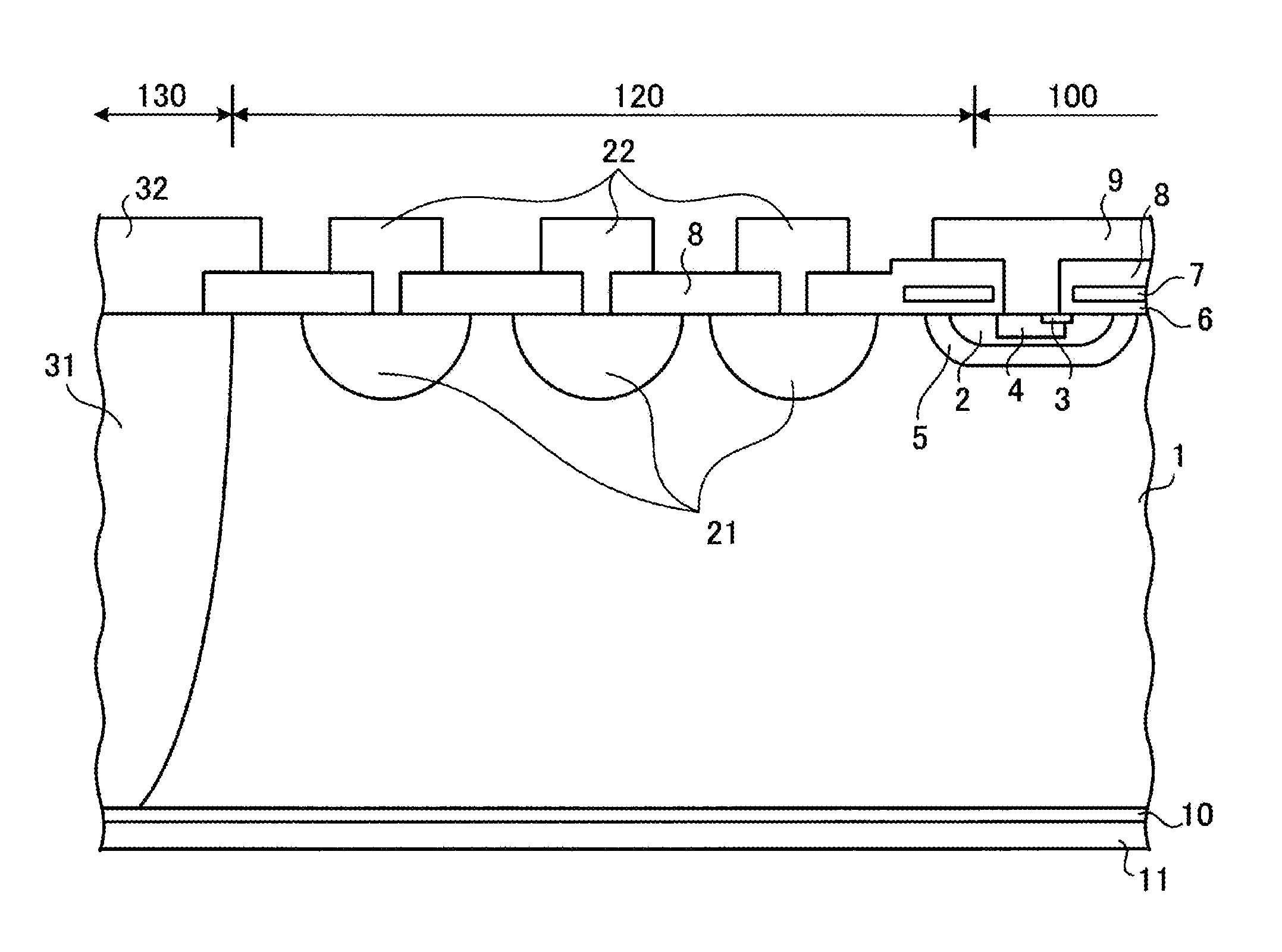
FIG. 1 is the cross sectional view of a reverse blocking IGBT according to the invention.

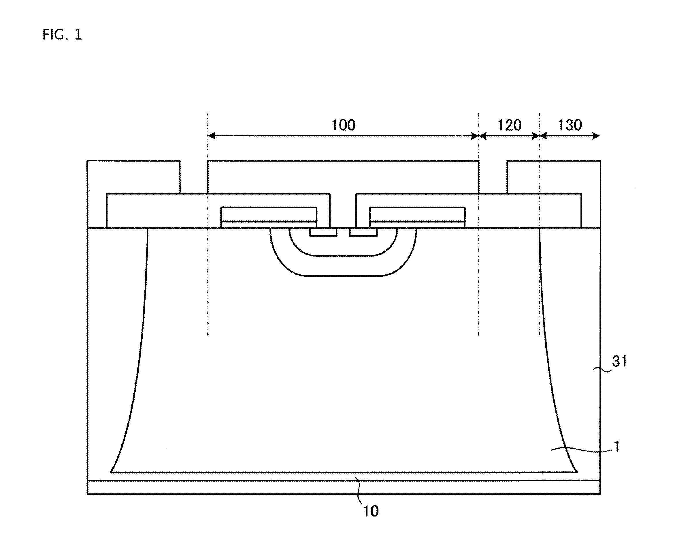
Referring now to FIG. 1, the reverse blocking IGBT according to the invention includes a semiconductor substrate working for n−-type (first conductivity type) drift region 1; active region 100 in the semiconductor substrate; breakdown withstanding region 120 outside active region 100; and separation section 130 outside breakdown withstanding region 120. It is effective for the semiconductor substrate to be 90 μm in thickness or thicker so as not to adversely affect the performances of the reverse blocking IGBT of the 600 V breakdown voltage class. In active region 100, a vertical IGBT structure is formed. The vertical IGBT structure includes an emitter-gate region formed on the front surface side of drift region 1 and p-type (second conductivity type) collector region 10 on the back surface side of drift region 1. Active region 100 will be described later in detail.

Drift region 1 corresponds to ...


PUM


Abstract

A semiconductor device according to embodiments of the invention includes an n-type drift region; a p-type base region formed selectively in the surface portion of the drift region; an n+-type emitter region and a p+-type body region, both formed selectively in the surface portion of base region; and an n-type shell region between the drift region and the base region, a shell region surrounding the entire region below base region. The shell region is doped more heavily than the drift region. The shell region contains an n-type impurity at an effective impurity amount of 8.0×1011 cm−2 or smaller. A drift region exhibits a resistivity low enough to prevent the depletion layer expanding from collector region, formed on the back surface of the drift region, toward a shell region from reaching the shell region.

Description

BACKGROUNDThe present invention relates to a semiconductor device.In the field of electric power converters using a semiconductor device, matrix converters have been known to the persons skilled in the art as direct converter circuits which conduct an alternating current to alternating current conversion (hereinafter referred to an “AC / AC conversion”), an alternating current to direct current conversion (hereinafter referred to an “AC / DC conversion”) and a direct current to alternating current conversion (hereinafter referred to a “DC / AC conversion”) without employing any DC smoothing circuit including an electrolytic capacitor and a DC reactor.The matrix converter includes AC switches. Since an AC voltage is applied to the AC switches, it is required for the AC switches to exhibit withstand voltages in the forward and reverse directions. In other words, the AC switches are required to exhibit a forward withstand voltage and a reverse withstand voltage. From the view points of reduc...

Claims


Application Information

Patent Timeline
Patent Type & Authority Applications(United States)
IPC IPC(8): H01L29/739
CPCH01L29/0619H01L29/7395H01L29/404
Inventor YOSHIKAWA, KOH
Owner FUJI ELECTRIC CO LTD
Why Eureka
Try Eureka