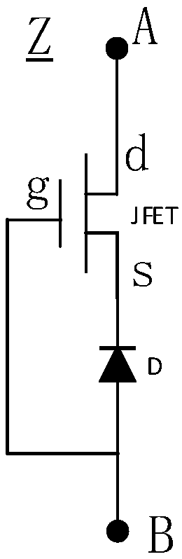
Combined switch

A combination switch and field effect transistor technology, applied in the direction of diodes, circuits, semiconductor devices, etc., can solve the problems of high forward conduction voltage, large reverse leakage current, high switching frequency, etc., and achieve high reverse withstand voltage and low forward voltage. The effect of directing the conduction voltage and increasing the switching rate

Inactive Publication Date: 2018-02-16
FSP POWERLAND TECH
View PDF3 Cites 3 Cited by
  • Summary
  • Abstract
  • Description
  • Claims
  • Application Information

AI Technical Summary

Problems solved by technology

Schottky diodes have the advantages of high switching frequency and forward voltage drop, but their biggest disadvantages are their low reverse bias voltage and large reverse leakage current, such as Schottky diodes made of silicon and metal. The reverse bias rated withstand voltage is only up to 200V, there is no Si-based Schottky diode between 200 and 600V, the withstand voltage of SiC Schottky diode is only 600 / 650V / 1200V, and there is no SiC Schottky below 600V Diode, and the forward voltage drop is very high
The reverse leakage current value has a positive temperature characteristic, and it tends to increase rapidly as the temperature rises. It is necessary to pay attention to the hidden danger of thermal runaway in practical design.

Method used


Image

  • Combined switch

Examples


Embodiment Construction

[0022] In order to make the purpose and technical solutions of the embodiments of the present invention more clear, the technical solutions of the embodiments of the present invention will be clearly and completely described below in conjunction with the drawings of the embodiments of the present invention. Apparently, the described embodiments are some, not all, embodiments of the present invention. Based on the described embodiments of the present invention, all other embodiments obtained by persons of ordinary skill in the art without creative efforts shall fall within the protection scope of the present invention.

[0023] "First", "second", "third", etc., if any, described in the present invention are used to distinguish between similar elements, and do not necessarily describe a specific order or chronological order. It is to be understood that the terms so used are interchangeable under appropriate circumstances such that the embodiments of the subject matter described ...


PUM


Abstract

The invention discloses a combined switch. The combined switch comprises a junction field effect transistor and a diode. The junction field effect transistor comprises a gate electrode, a source electrode and a drain electrode; the diode comprises an anode and a cathode; the drain electrode of the junction field effect transistor is a first terminal of the combined switch; the source electrode ofthe junction field effect transistor is connected with the cathode of the diode; the gate electrode of the junction field effect transistor is connected with the anode of the diode; and the anode of the diode is a second terminal of the combined switch. Compared to a single diode, the combined switch disclosed by the invention has a higher reverse withstand voltage, and has zero reverse recovery characteristic and a lower forward turn-on voltage.

Description

technical field [0001] The present invention relates to the field of power supplies, and in particular to fast recovery switches. Background technique [0002] Fast recovery diode (FRD for short) is a semiconductor diode with good switching characteristics, short reverse recovery time or zero reverse recovery. It is mainly used in switching power supplies, PWM pulse width modulators, frequency converters and other electronic devices. In the circuit, it is used as a high-frequency rectifier diode, a freewheeling diode or a damping diode. The internal structure of the fast recovery diode is different from the ordinary PN junction diode. It belongs to the PIN junction diode, that is, the base region I is added between the P-type silicon material and the N-type silicon material to form a PIN silicon chip. Because the base region is very thin and the reverse recovery charge is very small, the reverse recovery time of the fast recovery diode is short, the forward voltage drop is ...

Claims


Application Information

Patent Timeline
Patent Type & Authority Applications(China)
IPC IPC(8): H03K17/74
CPCH03K17/74
Inventor 徐明孙巨禄彭晗刘建
Owner FSP POWERLAND TECH
Why Eureka
Try Eureka