Decorative film and in mode decoration/forming process
a technology of decoration film and in-mode decoration/forming process, which is applied in the direction of instruments, bandages, other domestic objects, etc., can solve the problems of low yield rate of imd process, inability to improve the quality of overall product, and constructive interference of incident light, and achieves superior formability
- Summary
- Abstract
- Description
- Claims
- Application Information
AI Technical Summary
Benefits of technology
Problems solved by technology
Method used
Image
Examples
first embodiment
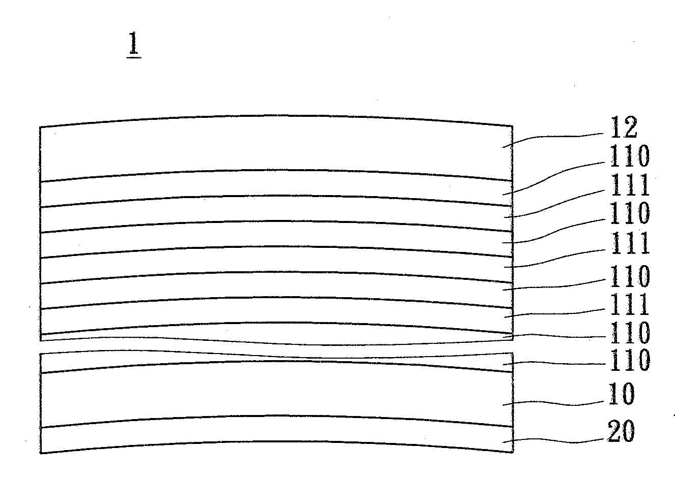
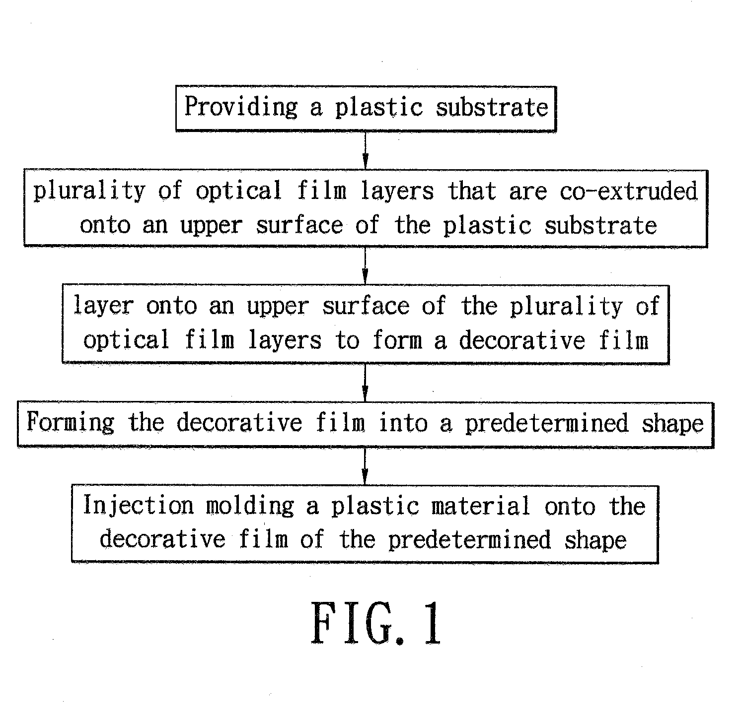
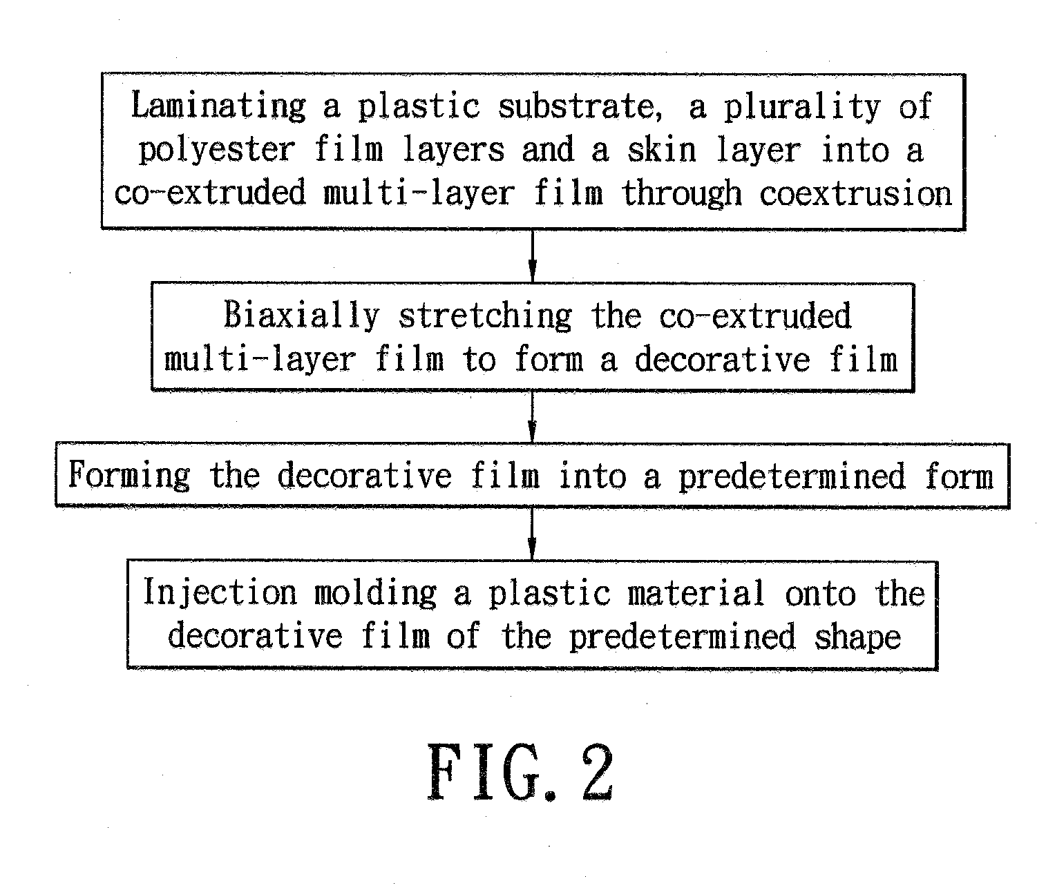
[0019]Referring now to FIGS. 1 and 2, the present invention provides a decorative film and an In Mode Decoration / Forming (IMD) process. By applying a plurality of optical film layers having differences in refractive indices and exhibiting superior formability to enclosures of electronic products such as cell phones, the IMD process imparts to the enclosures of electronic products an effect of changing colors with different viewing angles or a specular reflection effect. Through the following embodiments, the present invention can apply the plurality of optical film layers to the IMD process. The first embodiment comprises the following steps of (referring to FIGS. 3 to 3B together):
[0020]Step 1: a plastic substrate 10 having an upper surface and a lower surface, a plurality of optical film layers made of at least two different materials (i.e., the first resin film layers 110 and the second resin film layers 111), a skin layer 12 and a plastic material 20 are provided. The plastic su...
second embodiment
[0044]Next, the second embodiment is utilized to fabricate an enclosure having a mirror effect as follows. A 1050 μm thick decorative film having 304 layers is produced, through coextrusion, from a plastic substrate 10 made of polycarbonate, PEN materials and PMMA materials, and a skin layer 12 made of PMMA, in which the skin layer 12 made of PMMA is 40 μm in thickness and the plastic substrate 10 made of polycarbonate is 750 μm in thickness. The skin layer 12 used in this experiment group is made of a modified PMMA material which, through the aforesaid stretching and orientation, may get a hardness of at least 2H to effectively improve the protection capability. FIG. 4 shows a reflectance spectrum of this product. As shown in FIG. 4, the reflection band thereof falls within the visible light region, so the product presents a mirror appearance that is totally reflective at a front viewing angle of 0°, and as the viewing angle becomes larger, the reflection band shifts towards the sh...
PUM
| Property | Measurement | Unit |
|---|---|---|
| Temperature | aaaaa | aaaaa |
| Pressure | aaaaa | aaaaa |
| Hardness | aaaaa | aaaaa |
Abstract
Description
Claims
Application Information


