

Film formation method and storage medium
- Summary
- Abstract
- Description
- Claims
- Application Information
AI Technical Summary
Benefits of technology
Problems solved by technology
Method used
Image

Examples
embodiments
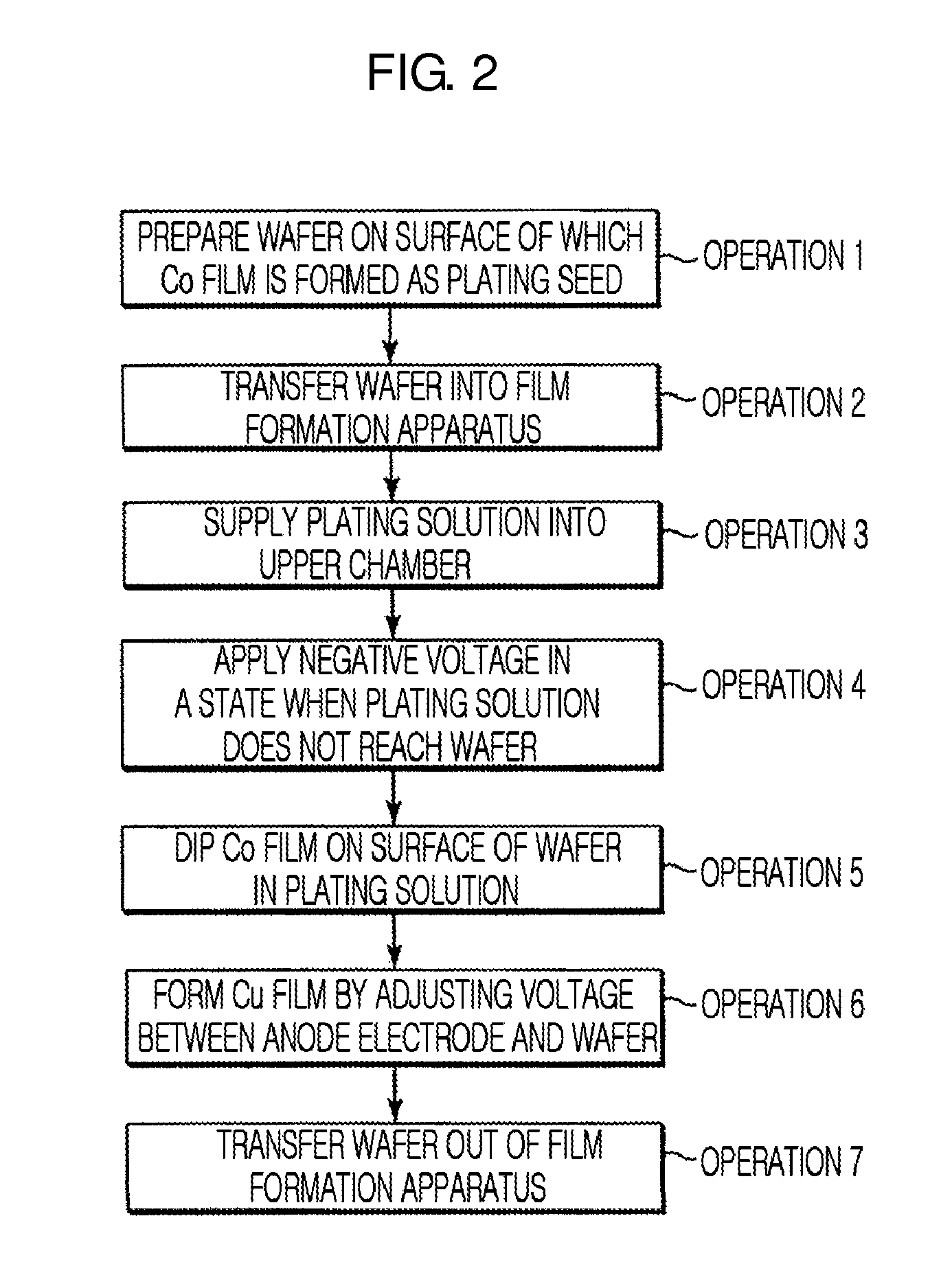
[0054]Next, embodiments will be explained.
[0055]A sample in which a Co film was formed as a plating seed to a thickness of 10 nm on a substrate and two samples in each of which a Co film was formed as a plating seed to a thickness of 5 nm on a substrate were prepared. First, no voltage was applied to the sample in which the Co film was formed to the thickness of 10 nm and one of the samples in which the Co film was formed to the thickness of 5 nm before the samples were dipped in plating solutions, and Cu films are formed by electroplating. Also, a voltage of −20 V was applied to the other sample in which the Co film was formed to the thickness of 5 nm before the sample was dipped in a plating solution, thereby a Cu film is formed by electroplating.
[0056]FIG. 7 are photographs showing plating states of the samples as time passes. As shown in FIG. 7, it was found that in the sample in which the Co film was formed to the thickness of 10 nm, the Cu film was formed satisfactorily althou...
PUM
| Property | Measurement | Unit |
|---|---|---|
| Thickness | aaaaa | aaaaa |
| Electric potential / voltage | aaaaa | aaaaa |
| Surface potential | aaaaa | aaaaa |
Abstract
Description
Claims
Application Information