Fast nanoimprinting apparatus using deformale mold

a nano-imprinting and mold technology, applied in the field of fast nano-imprinting apparatus using deformale molds, can solve the problems of not reaching the stage ready to meet the much higher requirements of industrial use, the cost of electron beam lithography to make the mold is averaged, and the nano-scale pattern writing speed of electron beam lithography is very slow

Active Publication Date: 2011-07-28
NANONEX
View PDF6 Cites 33 Cited by
  • Summary
  • Abstract
  • Description
  • Claims
  • Application Information

AI Technical Summary

Problems solved by technology

Previously, electron beam lithography is very slow to write nanoscale patterns.
Because the mold is repeatedly used for many cycles of imprinting, the high cost of using electron beam lithography to make the mold is averaged into these many imprints.
In overall, nanoimprint lithography has evolved into being a widely used technology for research laboratories, but not reached a stage ready to meet much higher requirements of industrial use.
Thus, throughput of the apparatus, which is defined as time consumption to finish a cycle of imprinting, is severely degraded by time cost of transferring among these different sites.
Furthermore, the internal transferring increases mechanical complexity of the apparatus and potentially introduces mechanical failure during operation.

Method used


Image

  • Fast nanoimprinting apparatus using deformale mold
  • Fast nanoimprinting apparatus using deformale mold
  • Fast nanoimprinting apparatus using deformale mold

Examples


Embodiment Construction

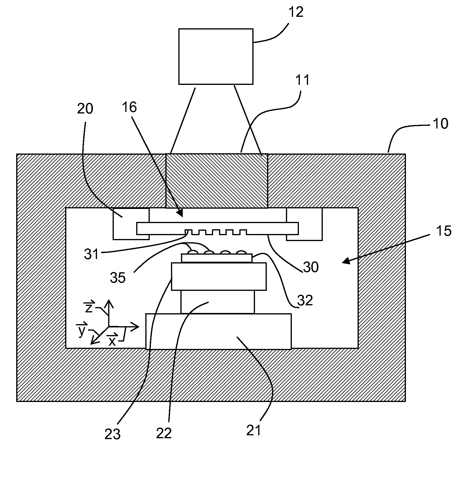
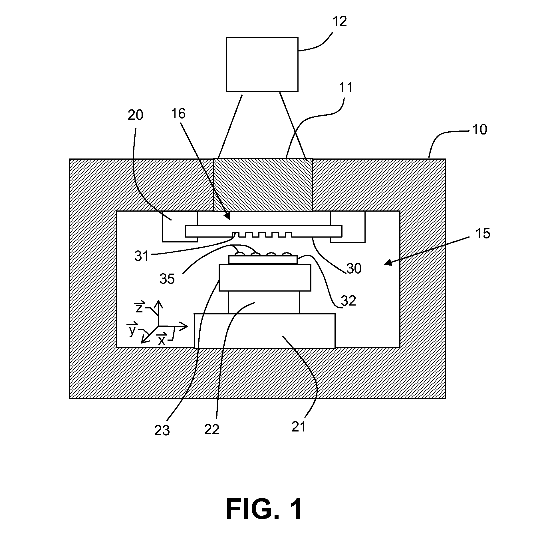
[0016]The descriptions assume that UV curable imprint is conducted if it is not clearly identified and UV curable imprint is used as example. However, the invention does not limit for UV curable imprint and also apply for thermo-plastic imprint. An ordinary skilled in the art who is familiar with nanoimprint technology can easily revise the embodiment described in the invention to implement the concept of the invention for all type of imprinting.

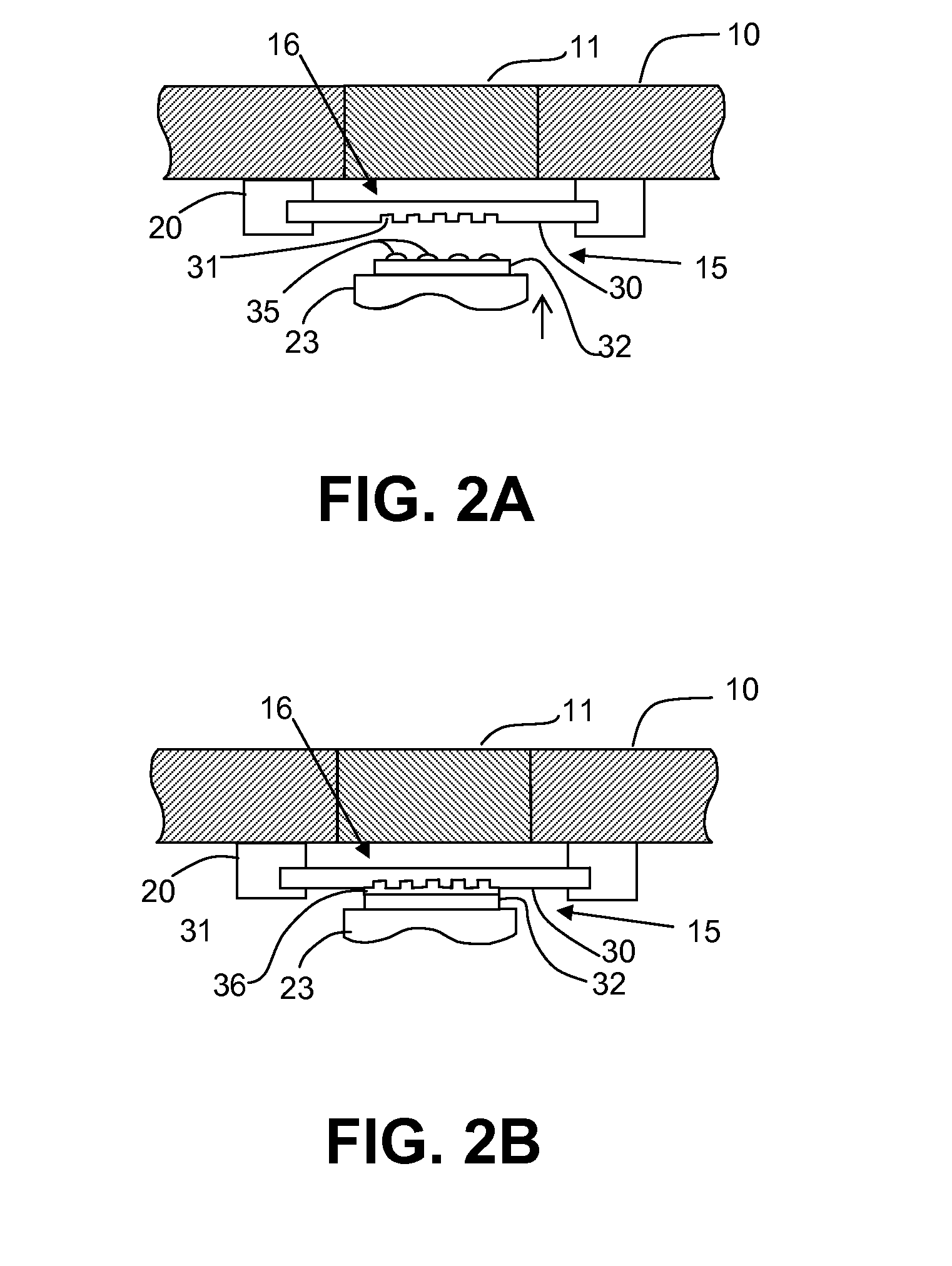
[0017]In accordance with the concept of the invention, referring to FIG. 1, the apparatus has a chamber 10 that can achieve vacuum or pressure inside. The top wall of the chamber has a light passing through section 11. Section 11 could be a transparent window made of quartz or glass. The section is able to hold vacuum seal and built-up pressure inside the chamber during operation. Section 11 allows a UV light passing through to provide UV curing exposure for UV curable imprint and a visible light passing through to view inside of the chamber...


PUM

PropertyMeasurementUnit
thicknessaaaaaaaaaa
thicknessaaaaaaaaaa
diameteraaaaaaaaaa

Abstract

The invention disclosed apparatuses and methods to do nanoimprint lithography using a deformable mold. Generally, the apparatus has a chamber with a transparent section on its top wall, which is capable of vacuuming and pressurizing. The deformable mold fixed firmly onto a hollow mold holder around its full periphery is attached to top inner surface of the chamber and positioned underneath the transparent section. The central area of the mold is freely accessible from underneath through the opening of the mold holder. An enclosed volume referring to mold mini-chamber is formed between the mold / holder and top wall of the chamber. Inside chamber, a stage assembly is installed. A chuck to vacuumly hold a substrate is mounted on top of the stage assembly. At beginning of the imprinting, the substrate with a layer of resist is positioned underneath the mold at a predetermined gap between them. Then, the substrate is moved up to contact with the mold either under vacuum or under atmosphere. The substrate and mold may be pressed further by introducing higher pressure inside the chamber. After consolidating the resist, the substrate is separated from the mold by either direct pull-down enabled by stage movement or deforming the mold enabled by differential pressure between the mold mini-chamber and the bulk volume of the chamber, or mixing of both.

Description

CROSS-REFERENCE FOR RELATED APPLICATIONS[0001]This application claims the benefit of U.S. Provisional Application Ser. No. 61 / 297,398 filed on Jan. 22, 2010, which is incorporated herein by reference.STATEMENT REGARDING FEDERALLY SPONSORED RESEARCH[0002]Not Applicable.FIELD OF INVENTION[0003]This invention relates to methods and apparatus for imprint lithography. It is particularly useful for providing fast replication of patterns of a mold having microscale or nanoscale features by imprint lithography.BACKGROUND OF THE INVENTION[0004]Nanoimprint lithography, also often called imprint lithography, is capable of replicating patterns on a pre-made mold as small as several nanometers. The pre-made mold has extruded areas and recessed areas on its replication surface, which constitute patterns of various shapes and sizes. The mold was typically made by a patterning step using electron beam lithography (EBL) or mixing of EBL and optical lithography, and, a follow-up etching step using re...

Claims


Application Information

Patent Timeline
Patent Type & Authority Applications(United States)
IPC IPC(8): B28B11/08B29C35/08B28B21/42B28B17/00
CPCB82Y10/00B82Y40/00B29L2007/001B29C59/02G03F7/0002
Inventor ZHANG, WEITAN, HUAHU, LINCHOU, STEPHEN Y.
Owner NANONEX
Why Eureka
Try Eureka