Touch panel and display device using the same

a display device and touch panel technology, applied in the field of touch panel, can solve the problems of increasing the signal connection line to a control circuit, the inability to detect input coordinates, and the electrode capacitance change hardly occurs, so as to prevent the cracking of the z electrode, the effect of increasing the electrostatic capacitan

Inactive Publication Date: 2011-07-28
PANASONIC LIQUID CRYSTAL DISPLAY CO LTD +1
View PDF5 Cites 35 Cited by
  • Summary
  • Abstract
  • Description
  • Claims
  • Application Information

AI Technical Summary

Benefits of technology

[0014]Still further, in the capacitive coupling type touch panel according to another aspect of the present invention, each of the plurality of Z electrodes may be arranged via spacers so as to be disposed at a certain distance from each of the plurality of X electrodes and each of the plurality of Y electrodes. In this case, compression that occurs under pressure applied by a touch causes an elastic layer laminated on the plurality of Z electrodes to be deformed along the shape of the spacers. As a result, the distance from the plurality of Z electrodes to the plurality of X electrodes, and the distance from the plurality of Z electrodes to the plurality of Y electrodes are reduced, which increases electrostatic capacitance. Accordingly, even when an input is made with nonconductive input means, the capacitance change occurring between the X electrodes and the Z electrodes, and between the Y electrodes and the Z electrodes (in a portion in which the distance between the electrodes changes by the pressure) may be detected, to thereby identify the coordinates of a touched position.
[0015]Still further, in the capacitive coupling type touch panel according to a further aspect of the present invention, a material for forming the Z electrodes may be formed on a thin nonconductive layer and bonded to the elastic layer, with a view toward preventing cracking of the Z electrodes that may occur due to compression that occurs under pressure applied by a touch when a material for forming the Z electrodes is directly formed on the elastic layer.

Problems solved by technology

Therefore, the capacitive coupling type touch panel has a problem that, in a case where a resin stylus, which is a nonconductive insulator used for a resistive touch panel or the like, is brought into contact with the capacitive coupling type touch panel, the capacitance change hardly occurs in the electrodes, and hence the input coordinates cannot be detected.
Further, the number of signal connection lines to a control circuit also increases, which leads to a reduction of reliability against impact or the like.
The number of terminals of the input processing part also increases to increase a circuit area, which leads to a fear of cost increase.
On the other hand, if a stylus having a tip end formed of a conductive rubber is used, the shape of the stylus needs to be 6 mm in diameter at a contact surface, provided that the number of the electrodes is unchanged, which brings an uncomfortable feeling in inputting characters.

Method used


Image

  • Touch panel and display device using the same
  • Touch panel and display device using the same
  • Touch panel and display device using the same

Examples


first embodiment

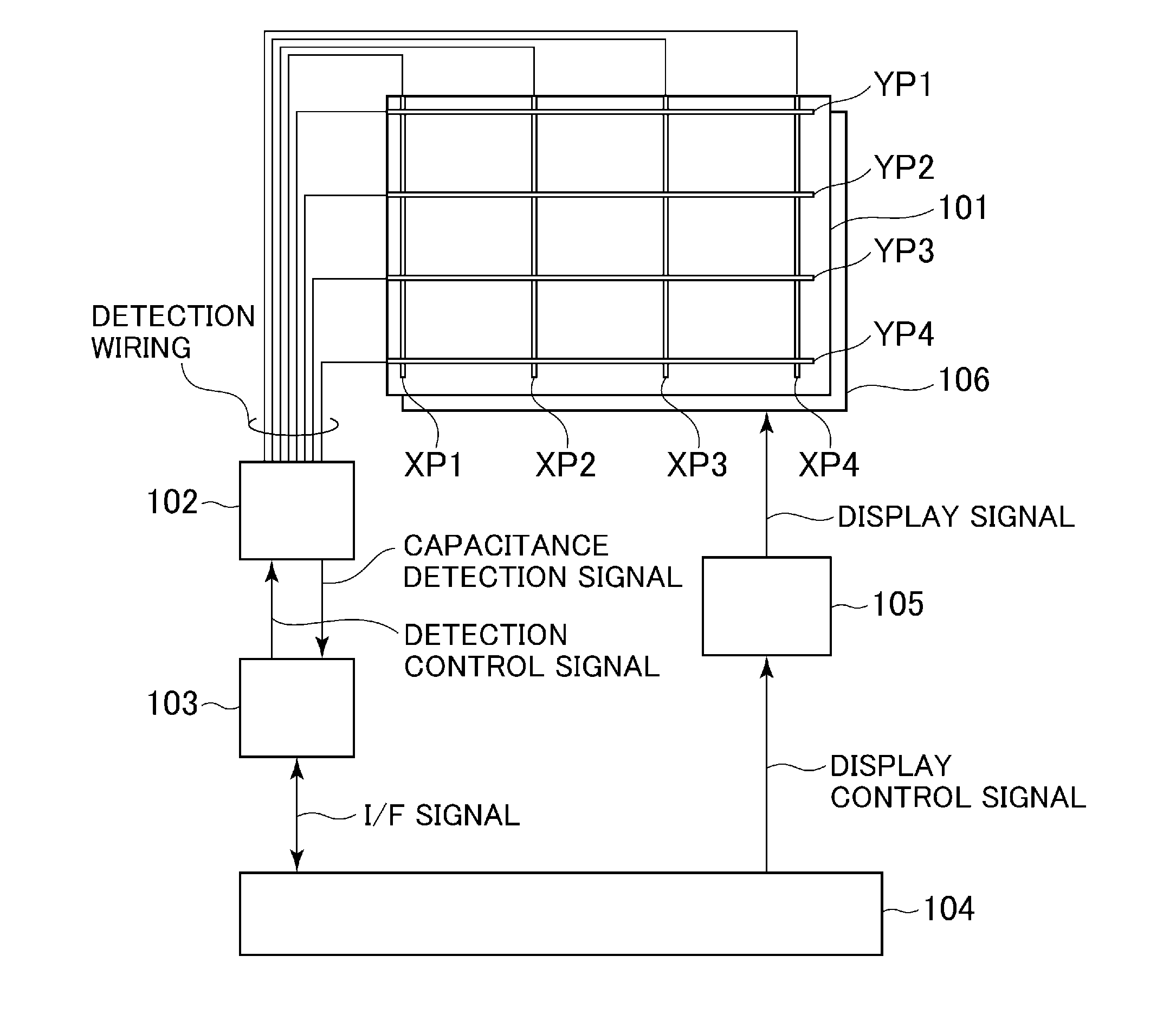
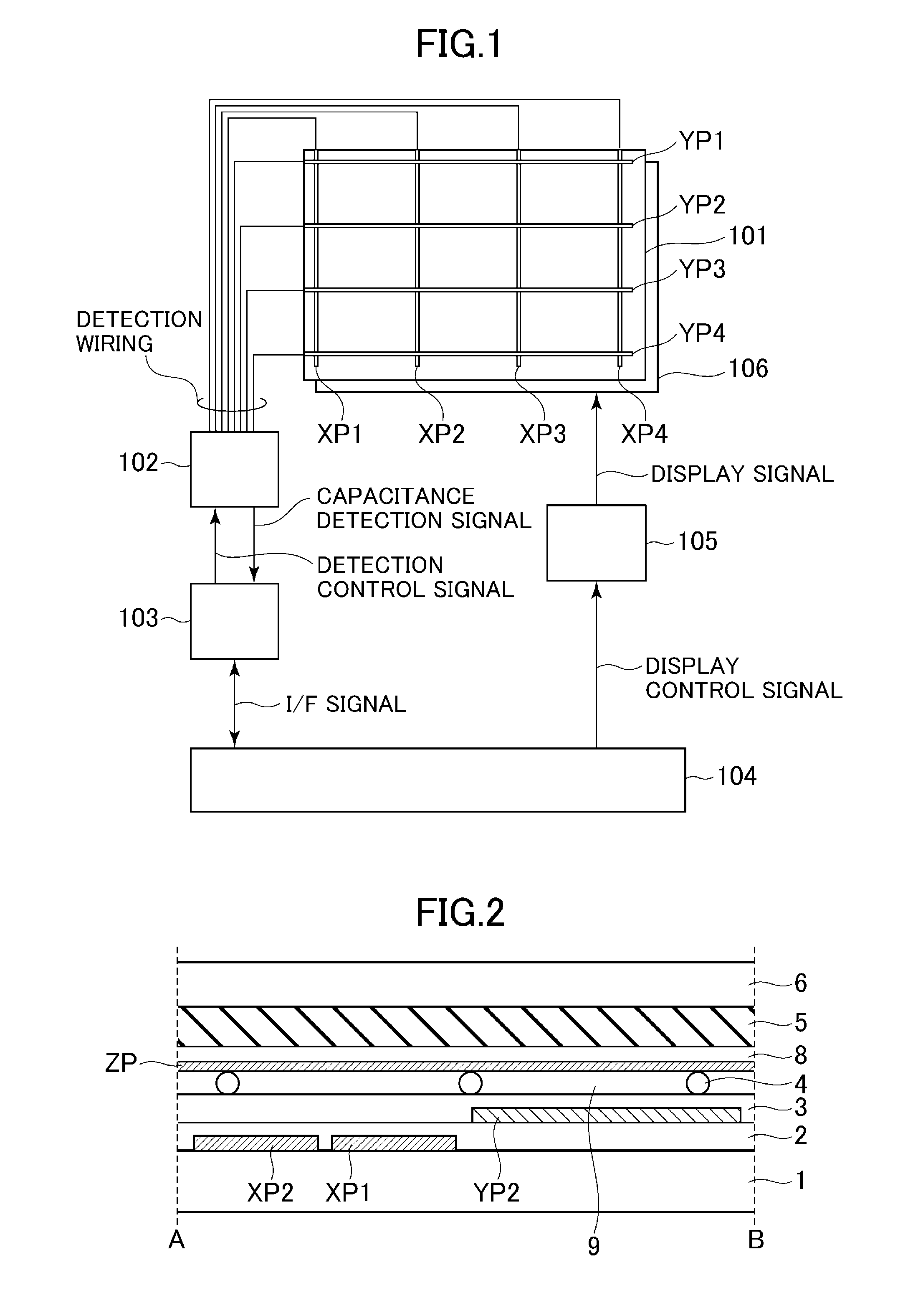
[0042]FIG. 1 illustrates a configuration of an input device (hereinafter, referred to as touch panel) according to a first embodiment of the present invention and a display device using the same.

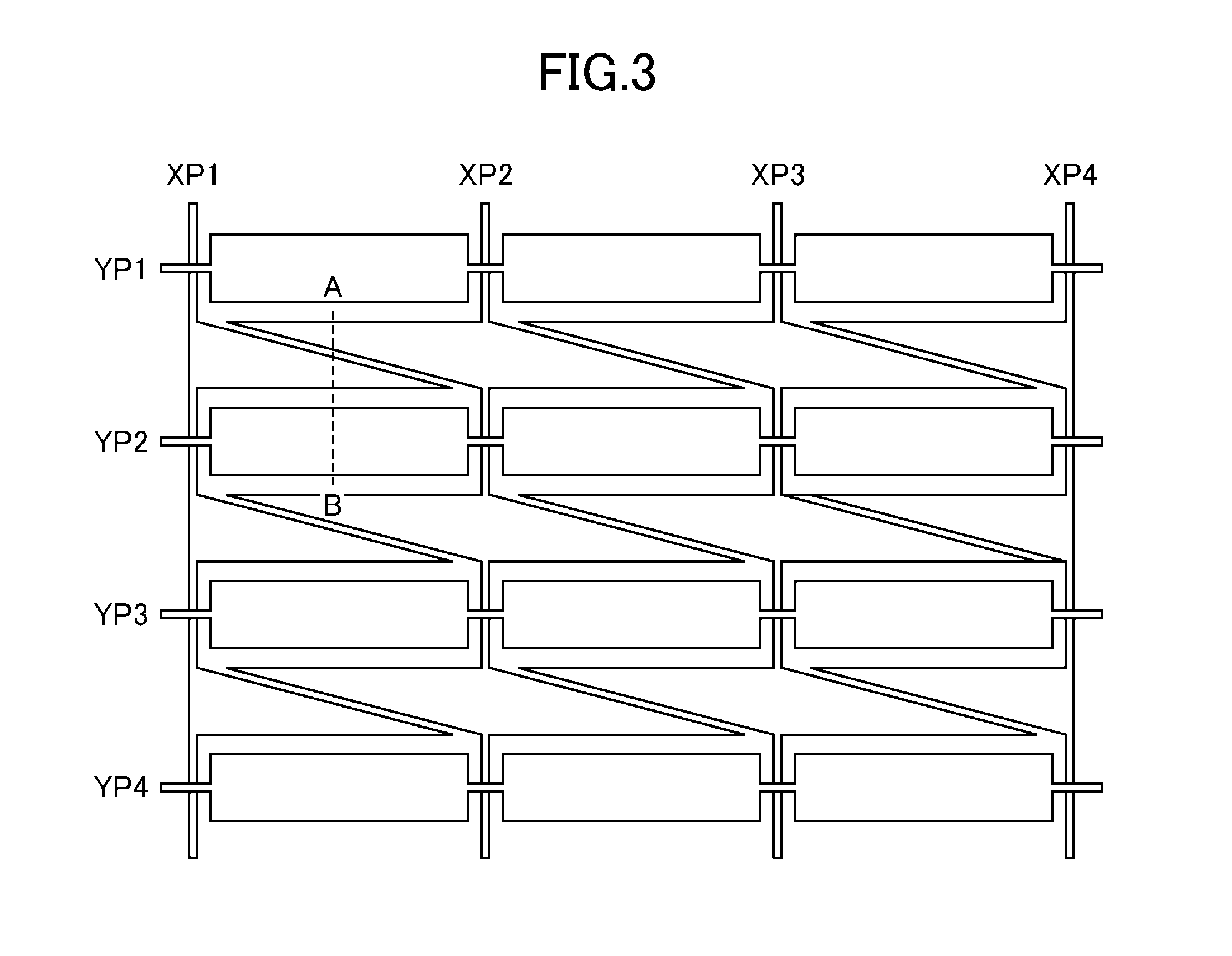
[0043]FIG. 1 illustrates a touch panel 101 according to the first embodiment of the present invention. The touch panel 101 includes X electrodes XP for capacitance detection and Y electrodes YP for capacitance detection. The first embodiment is described as an exemplary case where four X electrodes (XP1 to XP4) and four Y electrodes (YP1 to YP4) are provided. However, each of the numbers of the X electrodes XP and the Y electrodes YP is not limited to four.

[0044]The touch panel 101 is disposed on a front surface of a display portion 106 of the display device. Accordingly, when an image displayed on the display device is viewed by a user, the image displayed needs to pass through the touch panel 101, and hence the touch panel 101 is expected to have a high transmittance. The X electrodes XP a...

second embodiment

[0073]FIG. 6 is a configuration diagram of a touch panel 101 according to a second embodiment of the present invention, which illustrates a cross-sectional shape of the touch panel 101 taken along the line A-B of FIG. 3. The second embodiment is similar to the first embodiment in terms of material and property of each layer, and hence the description thereof is omitted herein.

[0074]The touch panel 101 according to the second embodiment of the present invention has a configuration in which the X electrode (transparent conductive film) XP, the first transparent insulating film 2, the Y electrode (transparent conductive film) YP, the second transparent insulating film 3, the transparent elastic layer 5, the nonconductive layer 8, the Z electrode ZP, and the spacers 4 for providing a space with respect to the Z electrode ZP are sequentially laminated on the first transparent substrate 1, with the second transparent substrate 6 being laminated on top thereof.

[0075]Next, a capacitance cha...

third embodiment

[0081]FIG. 8 is a configuration diagram of a touch panel 101 according to a third embodiment of the present invention, which illustrates a cross-sectional shape of the touch panel 101 taken along the line A-B of FIG. 3.

[0082]The touch panel 101 according to the third embodiment of the present invention has a configuration in which the X electrode (transparent conductive film) XP, the first transparent insulating film 2, the Y electrode (transparent conductive film) YP, the second transparent insulating film 3, and the spacers 4 for providing a space with respect to the Z electrode ZP, the Z electrode ZP, the nonconductive layer 8, and the transparent elastic layer 5 are sequentially laminated on the first transparent substrate 1, with the second transparent substrate 6 being laminated on top thereof.

[0083]The spacers 4 may be formed as dotted columnar spacers which are each made of a photo-curable resin material. The columnar spacers are formed as protrusions protruding from one of ...


PUM


Abstract

Provided is a capacitive coupling type touch panel, including: a plurality of coordinate detection electrodes (XP1, XP2, YP) for detecting X-Y position coordinates; a first substrate including the plurality of coordinate detection electrodes; and a second substrate (6) disposed to be opposed to the first substrate, in which: the capacitive coupling type touch panel further includes, between the first substrate (1) and the second substrate (6): a conductive layer (ZP) having conductivity; a nonconductive layer (8) supporting the conductive layer; a plurality of nonconductive spacers (4) that are formed at intervals in a plane direction of the first substrate and the second substrate; and an elastic layer (5) that is lower in rigidity than the first substrate, the second substrate, and the plurality of nonconductive spacers.

Description

CROSS-REFERENCE TO RELATED APPLICATION[0001]The present application claims priority from Japanese application JP2010-015270 filed on Jan. 27, 2010, the content of which is hereby incorporated by reference into this application.BACKGROUND OF THE INVENTION[0002]1. Field of the Invention[0003]The present invention relates to a touch panel for inputting coordinates on a screen and a display device using the same. In particular, the present invention relates to a touch panel of capacitive coupling type which enables an input using such an insulator as a resin pen, and to a display device using the touch panel.[0004]2. Description of the Related Art[0005]A display device including an input device (hereinafter, also referred to as “touch sensor” or “touch panel”) having an on-screen input function of inputting information to a display screen by a touch operation (contact and press operation, hereinafter, simply referred to as “touch”) with a user's finger or the like is used for mobile ele...

Claims


Application Information

Patent Timeline
Patent Type & Authority Applications(United States)
IPC IPC(8): G06F3/045
CPCG06F3/044G06F2203/04103G06F3/045G06F3/0446G06F3/0445G06F3/0447
Inventor SEKIGUCHI, SHINJI
Owner PANASONIC LIQUID CRYSTAL DISPLAY CO LTD
Why Eureka
Try Eureka