Connector device for building integrated photovoltaic device

a photovoltaic device and connector technology, applied in the direction of photovoltaic supports, coupling device connections, sustainable buildings, etc., can solve the problems of time-consuming and expensive installation, and achieve the effect of enhancing the serviceability of the device and easy electrical connection

Inactive Publication Date: 2011-07-28
DOW GLOBAL TECH LLC
View PDF21 Cites 51 Cited by
  • Summary
  • Abstract
  • Description
  • Claims
  • Application Information

AI Technical Summary

Benefits of technology

[0006]The present invention is directed to a solution to at least one or more of the issues described above. Particularly, the present invention seeks to provide a robust connector device and method that can more easily electrically connect a plurality of photovoltaic “PV” devices and / or locate these devices upon a building structure. It also may optionally provide some additional components (e.g. a bypass diode(s) and / or an indicator means) and may enhance the serviceability of the device.

Problems solved by technology

The roof / wall penetrations and / or extensive wiring can make installation time consuming and expensive.
Furthermore, when a system component (e.g. a single panel and / or a sub-component such as a bypass diode(s)) does become damaged or needs to be replaced, it may be valuable to have a connector that allows easy replacement of the PV system component or sub-component.

Method used


Image

  • Connector device for building integrated photovoltaic device
  • Connector device for building integrated photovoltaic device
  • Connector device for building integrated photovoltaic device

Examples


first embodiment

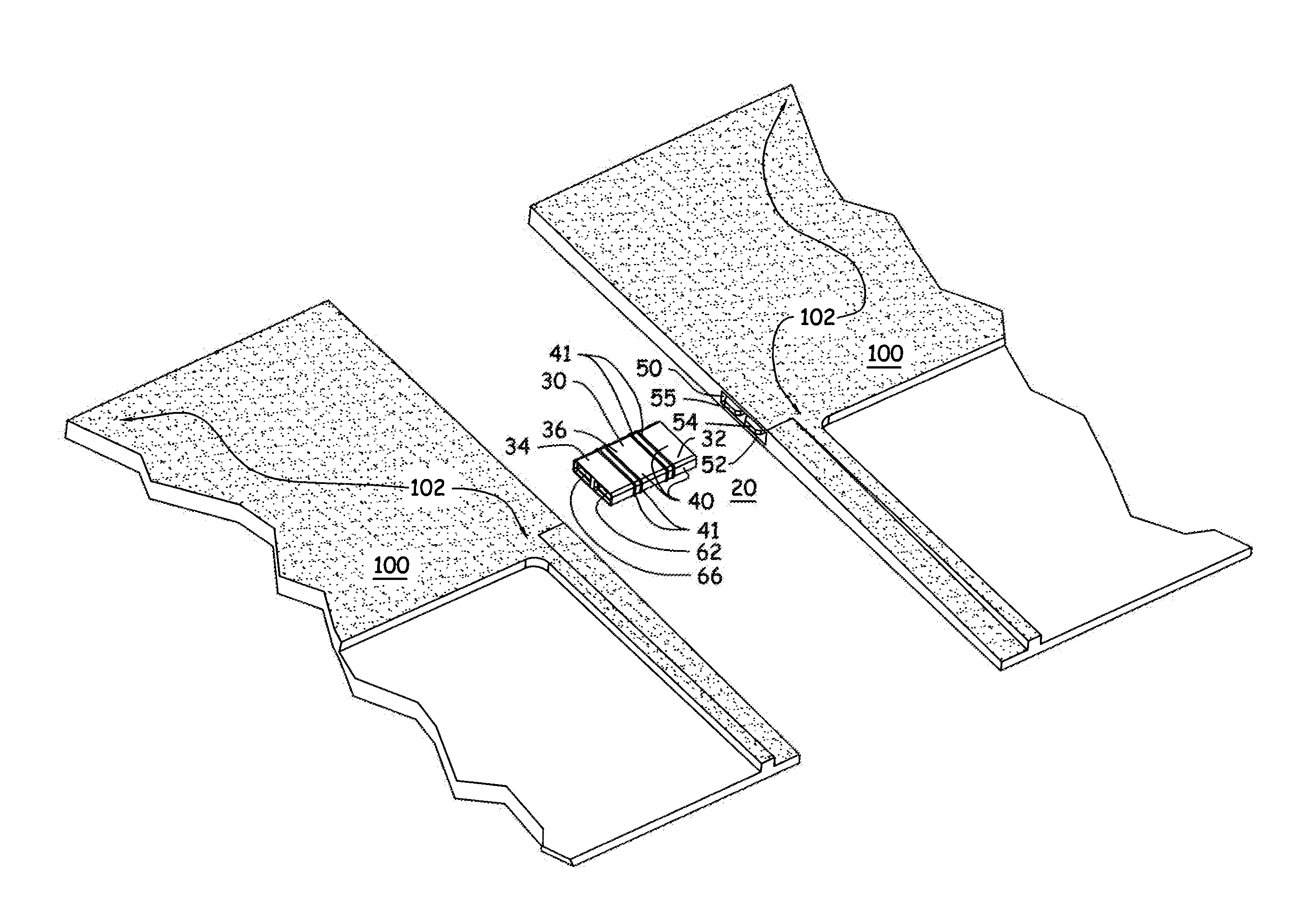
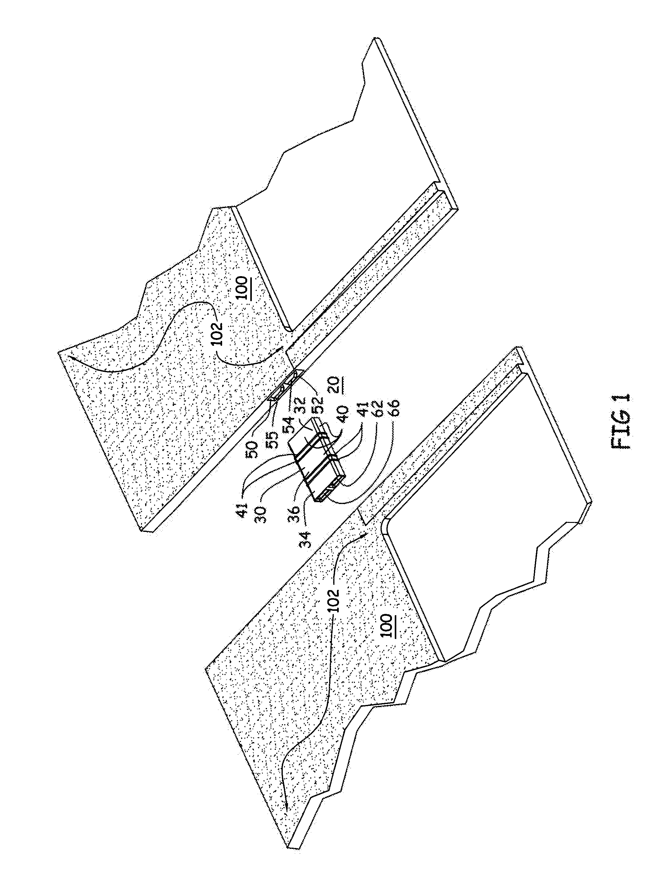
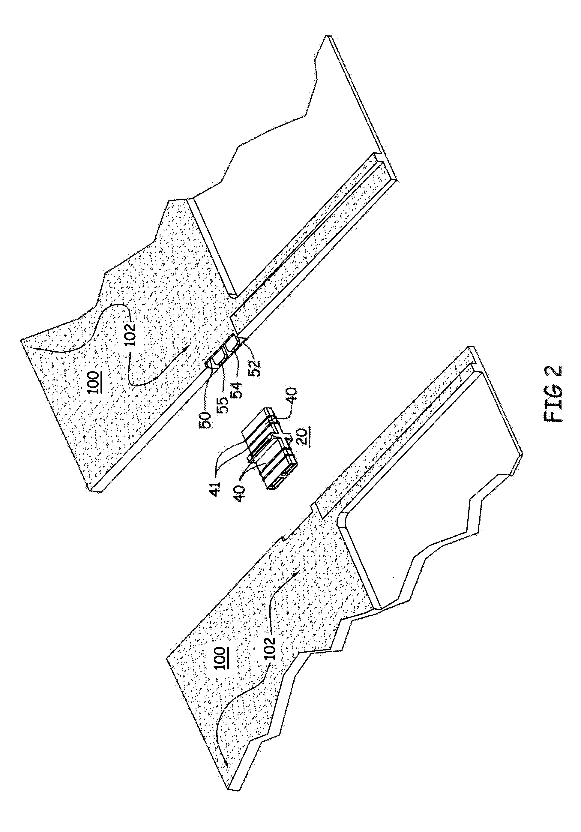
[0057]As in the first embodiment, it is also contemplated that the opposing receptacle connector housing 150 may be integral to an outer wall section 102 of the photovoltaic device 200. Also, the connector may include at least one bypass diode 64, a signaling device 39, and / or a second electrically conductive member 65.

[0058]The outwardly projecting locator portion 138 may be further described as projecting away from the outer surface 136 upward and / or downward towards a surface of the device 200. Preferably, projecting towards at least a top surface 201 of the device 200 and it is generally coplanar with the top surface 201, although it may be sub-flush or over-flush to the top surface 201.

[0059]It is contemplated that the arcuate bearing wall 139 of the outwardly projecting locator portion 138 functions to locate both the connector assembly 120 and at least two opposing receptacle connector housings 150. This in turn functions to help locate the opposing PV devices 200. The arcuat...

second embodiment

[0062]It is contemplated that at least one first locator portion 260 may be located in a peripheral wall portion 251 of the first receptacle connector housing 250. At least one second locator portion 360 may be located in a peripheral wall portion 351 of the second receptacle connector housing 350. Wherein the second locator portion 360 may be geometrically complementary with the first locator portion 260. Further wherein the first and second locater portions 260, 360 may provide a rotationally adjustable location function between the first and second photovoltaic devices 300. As in the second embodiment, the locator portions 260, 360 may include bearing walls 239, 339 and gapping segments 241, 341.

[0063]The connector assembly 220 may also include at least one receptacle electrical terminal 54 at least partially encapsulated in each of the first and second receptacle connector housings 250, 350. This terminal being electrically connected to the PV device 300.

[0064]The connector asse...

fifth embodiment

[0068]In the present invention, a method of locating and electrically connecting a plurality of photovoltaic devices together is contemplated. The method may include the steps of:

[0069]a. providing a first photovoltaic device with a first receptacle connector housing located on a side portion of the device, the receptacle connector housing including at least one first electrical connector terminal and at least one first locator feature; b. providing at least a second photovoltaic device with a second receptacle connector housing located on a side portion of the device, the second receptacle connector housing including at least one second electrical connector terminal and at least one second locator feature; c. providing a header connector according to any of the previously described embodiments; d. joining one end of the header connector to the first receptacle connector housing; e. joining the opposing end of the header connector to the second receptacle connector housing; f. rotat...


PUM

PropertyMeasurementUnit
thicknessaaaaaaaaaa
thicknessaaaaaaaaaa
thicknessaaaaaaaaaa

Abstract

The present invention is premised upon a connector device and method that can more easily electrically connect a plurality of PV devices or photovoltaic system components and / or locate these devices / components upon a building structure. It also may optionally provide some additional sub-components (e.g. at least one bypass diode and / or an indicator means) and may enhance the serviceability of the device.

Description

CLAIM OF PRIORITY[0001]The present application claims the benefit of the filing date of U.S. Provisional Application Nos. 61 / 050,341 (filed 5 May 2008); 61 / 098,941 (filed 22 Sep. 2008); 61 / 149,451 (filed 3 Feb. 2009), the contents of which are hereby incorporated by reference in their entirety.[0002]This invention was made with U.S. Government support under contract DE-FC36-07G01754 awarded by the Department of Energy. The U.S. Government has certain rights in this invention.FIELD OF THE INVENTION[0003]The present invention relates to an improved connector, more particularly to an improved connector for a photovoltaic device.BACKGROUND[0004]Efforts to improve photovoltaic (“PV”) systems, particularly to improve the connection, installation, and service of multiple devices are subject to continuing development within the PV industry. Of special interest are those PV systems that are integrated into building structures (e.g. roofing shingles, exterior wall coverings, or platforms). To...

Claims


Application Information

Patent Timeline
Patent Type & Authority Applications(United States)
IPC IPC(8): H01R13/62H01R13/64H01R43/00
CPCH01R13/055Y10T29/49117H01R31/00Y02B10/12H01L31/0508H01L31/18H01R12/79H01R13/639H02S40/34H02S40/36H01L31/048H01L31/05Y02E10/50Y10T29/49826Y10T29/49355H01R13/113H02S20/25H01R13/7032H02S20/23Y02A30/60Y02B10/10H02S20/00H01L31/02013H01L31/02008
Inventor KEENIHAN, JAMES R.LANGMAID, JOSEPH A.EURICH, GERALD K.LESNIAK, MICHAEL J.MAZOR, MICHAEL H.CLEEREMAN, ROBERT J.GASTON, RYAN S.
Owner DOW GLOBAL TECH LLC
Why Eureka
Try Eureka