Method and apparatus for using aerial image sensitivity to model mask errors

a technology of aerial image and model mask, applied in the field of integrated circuit design and fabrication, can solve the problems of reducing the efficacy of optical proximity correction (opc), negatively affecting the efficacy of downstream applications, and increasing the time-to-market of an integrated circui

Active Publication Date: 2011-07-28
SYNOPSYS INC
View PDF4 Cites 7 Cited by
  • Summary
  • Abstract
  • Description
  • Claims
  • Application Information

AI Technical Summary

Problems solved by technology

Inaccuracies in the process model negatively affect the efficacy of downstream applications.
For example, inaccuracies in the photolithography process model can reduce the efficacy of optica...

Method used


Image

  • Method and apparatus for using aerial image sensitivity to model mask errors
  • Method and apparatus for using aerial image sensitivity to model mask errors
  • Method and apparatus for using aerial image sensitivity to model mask errors

Examples


Embodiment Construction

[0024]The following description is presented to enable any person skilled in the art to make and use the invention, and is provided in the context of a particular application and its requirements. Various modifications to the disclosed embodiments will be readily apparent to those skilled in the art, and the general principles defined herein may be applied to other embodiments and applications without departing from the spirit and scope of the present invention. Thus, the present invention is not limited to the embodiments shown, but is to be accorded the widest scope consistent with the principles and features disclosed herein.

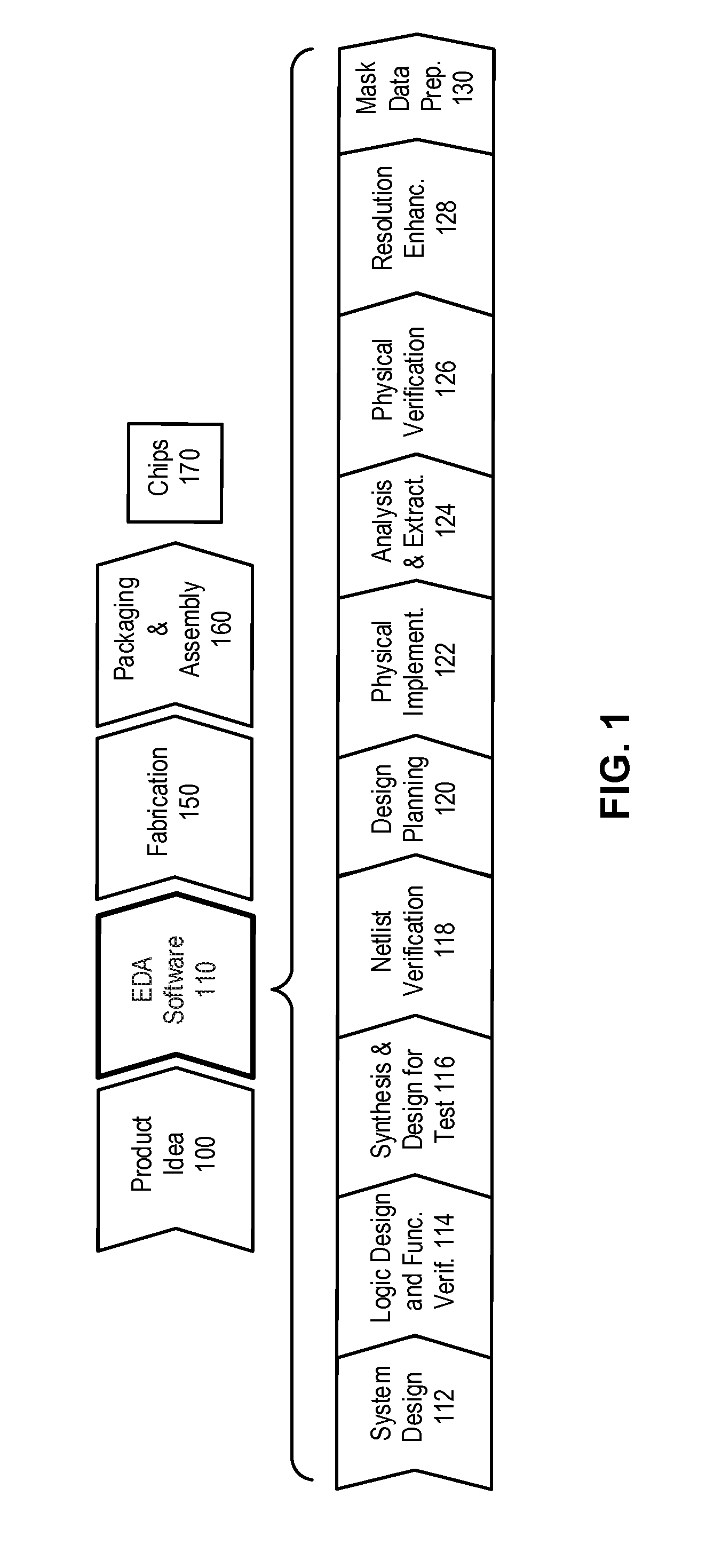
[0025]FIG. 1 illustrates various steps in the design and fabrication of an integrated circuit. The process starts with a product idea 100, which is realized using Electronic Design Automation (EDA) software 110. Chips 170 can be produced from the finalized design by performing fabrication 150 and packaging and assembly 160 steps.

[0026]A design flow that uses ...


PUM


Abstract

One embodiment of the present invention provides techniques and systems for modeling mask errors based on aerial image sensitivity. During operation, the system can receive an uncalibrated process model which includes a mask error modeling term which is based at least on an aerial image sensitivity to mask modifications which represent mask errors. Next, the system can fit the uncalibrated process model using measured CD data. Note that the mask error modeling term can also be dependent on the local pattern density. In some embodiments, the mask error modeling term can include an edge bias term and a corner rounding term. The edge bias term can be based on the sensitivity of the aerial image intensity to an edge bias, and the corner rounding term can be based on the sensitivity of the aerial image intensity to a corner rounding adjustment.

Description

BACKGROUND[0001]1. Technical Field[0002]The present invention relates to integrated circuit design and fabrication. More specifically, the present invention relates to methods and apparatuses for using aerial image sensitivity to model mask errors.[0003]2. Related Art[0004]Rapid advances in computing technology have made it possible to perform trillions of computational operations each second on data sets that are sometimes as large as trillions of bytes. These advances can be attributed to the dramatic improvements in semiconductor manufacturing technologies which have made it possible to integrate tens of millions of devices onto a single chip.[0005]As semiconductor design enters the deep submicron era, process model accuracy and efficiency is becoming increasingly important. Inaccuracies in the process model negatively affect the efficacy of downstream applications. For example, inaccuracies in the photolithography process model can reduce the efficacy of optical proximity correc...

Claims


Application Information

Patent Timeline
IPC IPC(8): G06F17/50
CPCG03F1/144G03F1/36G03F7/70625G03F7/705G03F7/70516G03F7/70441G03F1/68
Inventor FAN, YONGFAHUANG, JENSHENG
Owner SYNOPSYS INC
Why Eureka
Try Eureka