Field effect transistor (FET) and method of forming the fet without damaging the wafer surface

a field effect transistor and fet technology, applied in the field of fets, can solve the problems of increasing wafer surface damage, device formation, device performance, etc., and achieve the effect of selective selection

Inactive Publication Date: 2011-08-04
ALSEPHINA INNOVATIONS INC
View PDF10 Cites 13 Cited by
  • Summary
  • Abstract
  • Description
  • Claims
  • Application Information

AI Technical Summary

Benefits of technology

[0006]Also disclosed herein are embodiments of a method of forming such a planar FET structure on a semiconductor wafer such that the wafer surface, particularly, in the FET source / drain regions, remains essentially damage-free. Generally, the method can comprise providing a semiconductor layer. Next, a gate stack can be formed on the top surface of the semiconductor layer. Then, gate sidewall spacers can be formed on the opposing sidewalls of the gate stack, particularly, without damaging the adjacent wafer surface.
[0007]In order to form gate sidewall spacers without damaging the adjacent wafer surface, a blanket spacer material layer can be deposited such that it covers the gate stack and also covers the exposed top surface of the semiconductor layer adjacent to the gate stack. Next, the spacer material layer can be anisotropically etched (e.g., by a reactive ion etch (RIE) process), stopping just prior to exposing the top surface of the semiconductor layer such that horizontal portions of the spacer material layer remain on the top surface of the semiconductor layer and vertical portions of the spacer material layer remain on the opposing sidewalls of the gate stack. Since this etch process is anisotropic, the horizontal portions of the spacer material layer will be relatively thin as compared to the vertical portions. Following the anisotropic etch process, the spacer material layer is further isotropically etched (e.g., by a highly selective wet etch process), stopping upon complete removal of the relatively thin horizontal portions of the spacer material layer from the top surface of the semiconductor layer, but prior to complete removal of the relatively thick vertical portions of the spacer material layer from the opposing sidewalls of the gate stack, thereby forming the gate sidewall spacers. Since this etch process is isotropic and highly selective, the exposed portions of the top surface of the semiconductor layer adjacent to the gate sidewall spacers are not damaged when the horizontal portions of the spacer material layer are etched away.

Problems solved by technology

Conventional techniques for forming field effect transistor (FETs) on semiconductor wafers (e.g., a silicon-on-insulator (SOI) wafers, bulk silicon wafers, etc.) often result in damage to the wafer surface, particularly in the FET source / drain and source / drain extension regions.
As devices are scaled in size, wafer surface damage can have an increasingly significant impact on device formation and, ultimately, on device performance.

Method used


Image

  • Field effect transistor (FET) and method of forming the fet without damaging the wafer surface
  • Field effect transistor (FET) and method of forming the fet without damaging the wafer surface
  • Field effect transistor (FET) and method of forming the fet without damaging the wafer surface

Examples


Embodiment Construction

[0022]The embodiments of the invention and the various features and advantageous details thereof are explained more fully with reference to the non-limiting embodiments that are illustrated in the accompanying drawings and detailed in the following description.

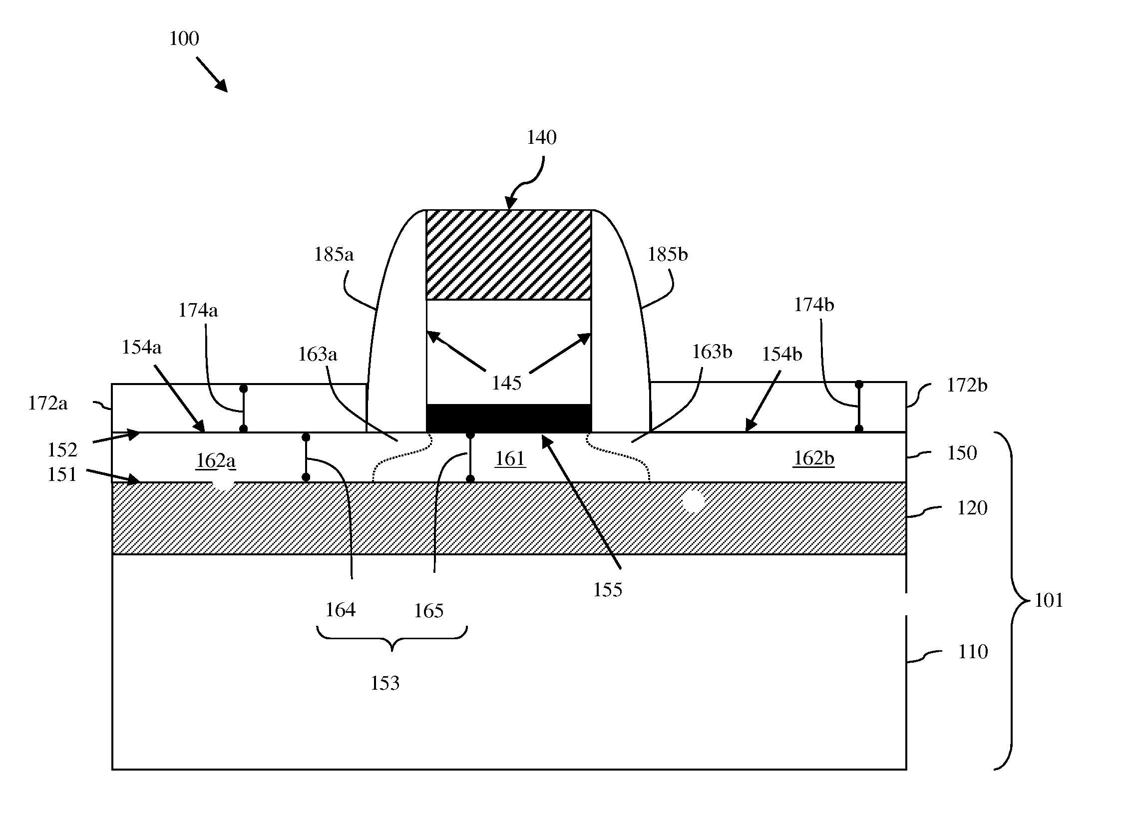
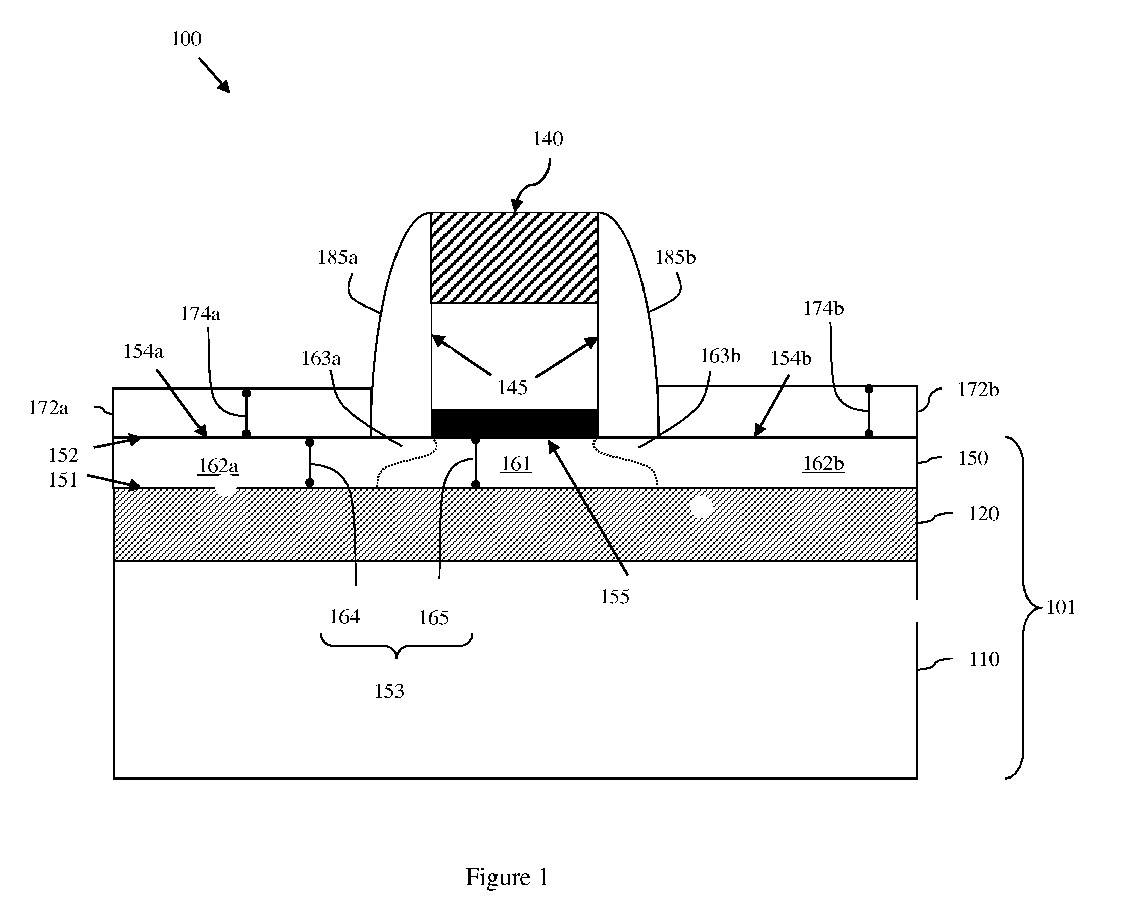
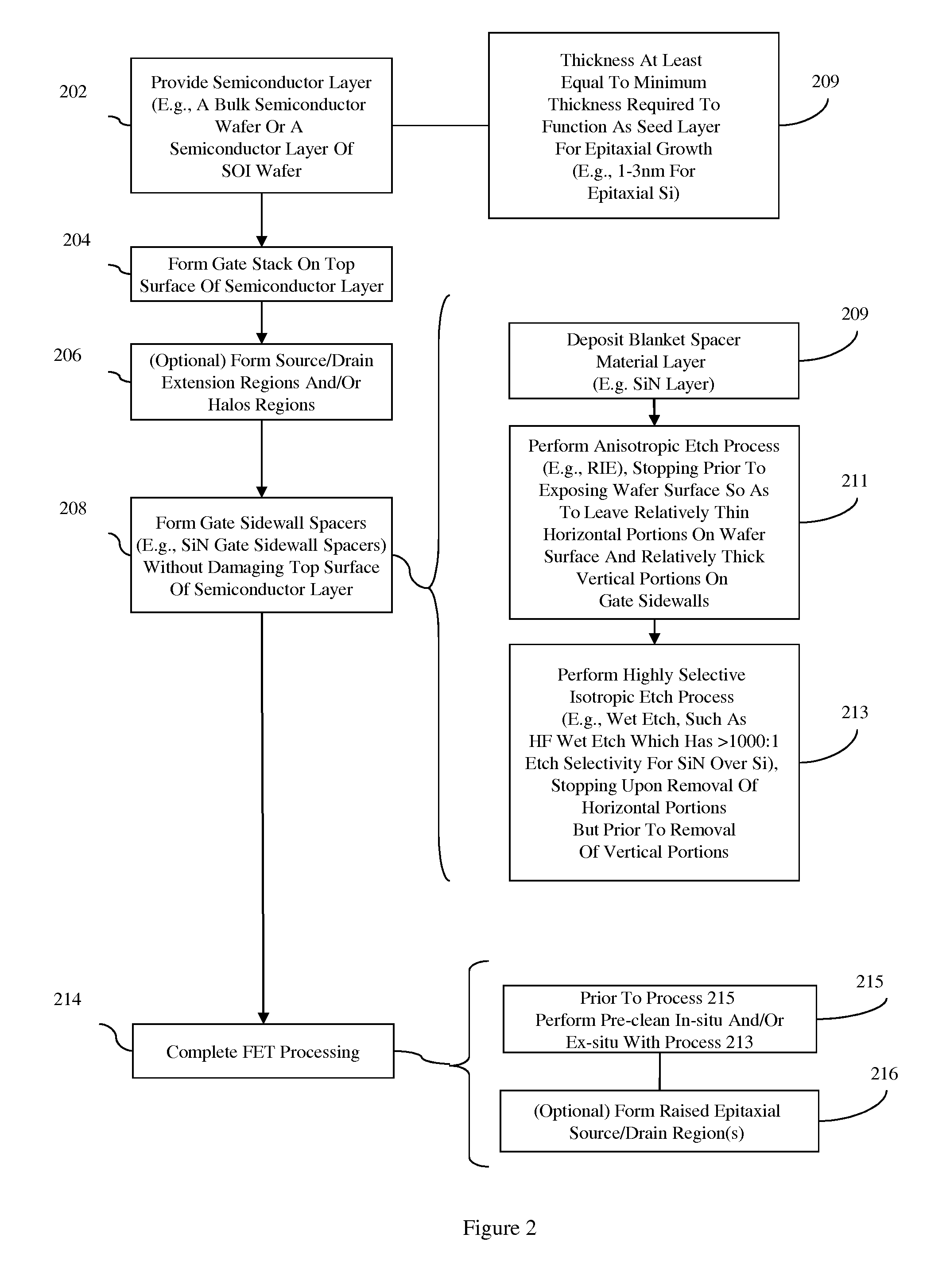
[0023]As mentioned above, conventional techniques for forming planar field effect transistor (FETs) on semiconductor wafers (e.g., a silicon-on-insulator (SOI) wafers, bulk silicon wafers, etc.) often result in damage to the wafer surface. Unfortunately, as devices are scaled in size, this wafer surface damage can have an increasingly significant impact on device formation and, ultimately, on device performance.

[0024]For example, it has been proposed that an extra-thin silicon-on-insulator (ETSOI) wafer could be used in order to provide a planar FET architecture suitable for the 22 nm technology node and beyond. An ETSOI wafer is a silicon-on-insulator (SOI) wafer comprising a semiconductor substrate 10, an insulator layer 20 ...


PUM


Abstract

Disclosed are a field effect transistor structure and a method of forming the structure. A gate stack is formed on the wafer above a designated channel region. Spacer material is deposited and anisotropically etched until just prior to exposing any horizontal surfaces of the wafer or gate stack, thereby leaving relatively thin horizontal portions of spacer material on the wafer surface and relatively thick vertical portions of spacer material on the gate sidewalls. The remaining spacer material is selectively and isotropically etched just until the horizontal portions of spacer material are completely removed, thereby leaving only the vertical portions of the spacer material on the gate sidewalls. This selective isotropic etch removes the horizontal portions of spacer material without damaging the wafer surface. Raised epitaxial source / drain regions can be formed on the undamaged wafer surface adjacent to the gate sidewall spacers in order to tailor source / drain resistance values.

Description

BACKGROUND[0001]1. Field of the Invention[0002]The embodiments of the invention generally relate to field effect transistors (FETs) and, more specifically, to a FET structure formed on a semiconductor wafer (e.g., a silicon-on-insulator (SOI) wafer, a bulk silicon wafer, etc.) and a method of forming the FET structure on a semiconductor wafer without damaging the wafer surface.[0003]2. Description of the Related Art[0004]Conventional techniques for forming field effect transistor (FETs) on semiconductor wafers (e.g., a silicon-on-insulator (SOI) wafers, bulk silicon wafers, etc.) often result in damage to the wafer surface, particularly in the FET source / drain and source / drain extension regions. As devices are scaled in size, wafer surface damage can have an increasingly significant impact on device formation and, ultimately, on device performance. Therefore, there is a need in the art for an improved FET structure and a method of forming the FET structure without damaging the semic...

Claims


Application Information

Patent Timeline
Patent Type & Authority Applications(United States)
IPC IPC(8): H01L29/78H01L21/28H01L21/336
CPCH01L29/78H01L21/28H01L29/6656H01L29/6653H01L29/66772H01L21/31116
Inventor CHENG, KANGGUODORIS, BRUCE B.ZHU, YU
Owner ALSEPHINA INNOVATIONS INC
Why Eureka
Try Eureka