Semiconductor device and method of fabricating the same

Inactive Publication Date: 2011-08-04
SK HYNIX INC
View PDF3 Cites 7 Cited by
  • Summary
  • Abstract
  • Description
  • Claims
  • Application Information

AI Technical Summary

Benefits of technology

[0019]An embodiment of the present invention is directed to a semiconductor device and a method for manufacturing the semiconductor device, which is configured to reduce a leakage current generated by parasitic field effects and to increase or improve operational reliability by forming an insulating layer inside a word line comprising recess gate patterns over a fin-type channel region included therein.

Problems solved by technology

As storage capacities of semiconductor memory have increased, the sizes of the semiconductor memory apparatus have not increased proportionally.
However, as the data storage capacity and the degree of integration of a semiconductor memory apparatus increase, the size of each unit cell is required to shrink.
As a result, a short channel effect and drain induced barrier lowering (DIBL) have occurred in the typical transistor, which deteriorates the operational reliability of the transistor.
As a result, it may cause the refresh property of the semiconductor memory apparatus to deteriorate.
For example, because of a neighbor gate effect, charges in a storage node tend to leak while a cell transistor is turned off (inactive).
That is, the neighbor gate effect causes an off leakage current so that dynamic refresh performance, related to refresh performance while a unit cell is under operation, gets worse.
Furthermore, a passing gate effect can increase a drain-induced-barrier-lowering (DIBL) phenomenon so that static refresh performance related to a data retention capability of the unit cell also gets worse.
These defects cause a decrease in production yield.

Method used


Image

  • Semiconductor device and method of fabricating the same
  • Semiconductor device and method of fabricating the same
  • Semiconductor device and method of fabricating the same

Examples


Embodiment Construction

[0036]Embodiments of the present invention will be described below in more detail with reference to the accompanying drawings. The present invention may, however, be embodied in different forms and should not be limited to the embodiments set forth herein. Rather, these embodiments are provided so that this disclosure will be thorough and complete, and will fully convey the scope of the present invention to those skilled in the art. Throughout the disclosure, like reference numerals refer to like parts throughout the various figures and embodiments of the present invention.

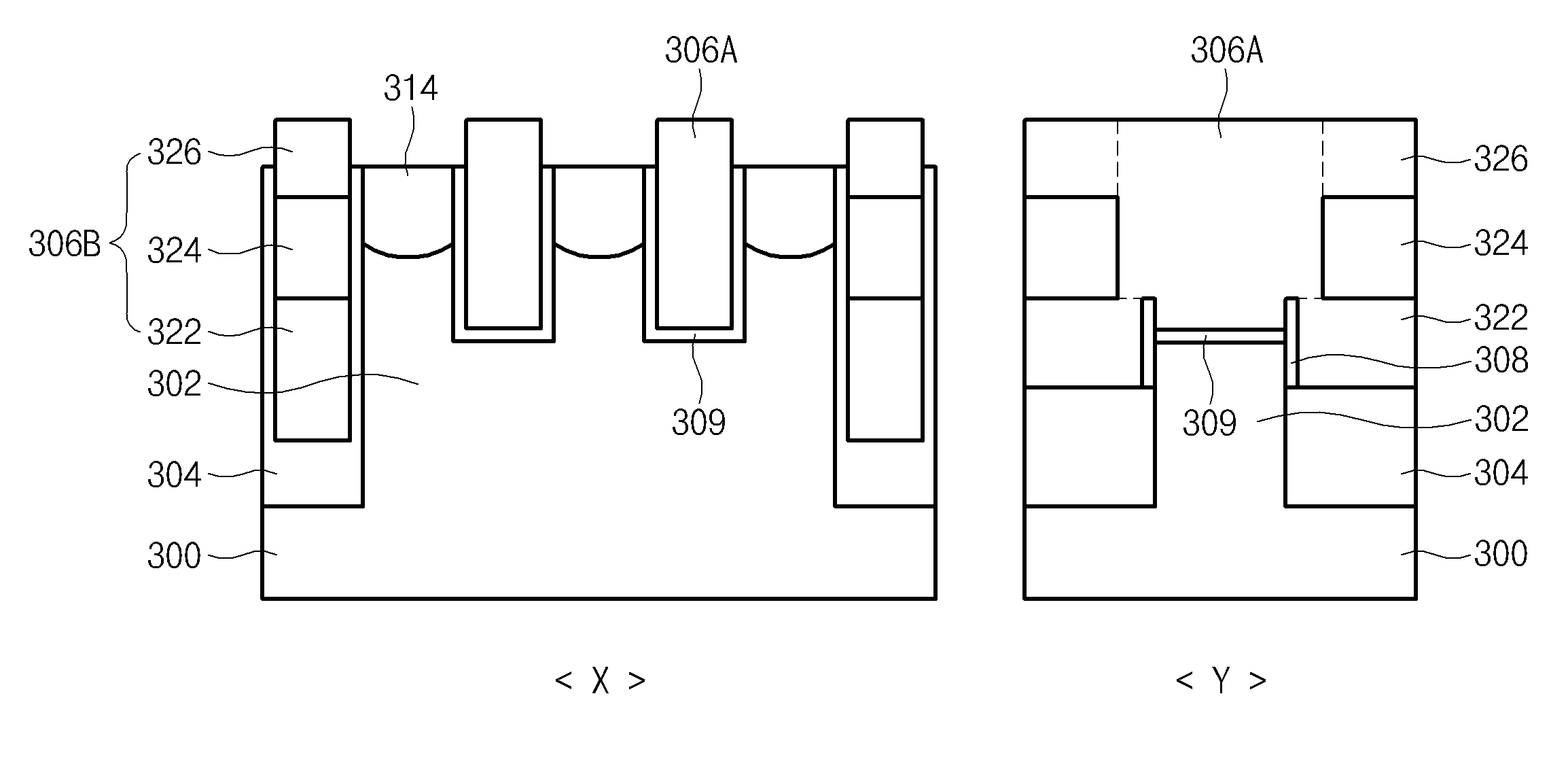
[0037]In an embodiment of the present invention, a word line includes two different-type gate patterns: one is a buried gate pattern formed over a device isolation layer; and the other is a recess gate pattern formed over an active region. Accordingly, a semiconductor apparatus comprising such gate patterns has the advantages of improving dynamic and static refresh performance and preventing an electrical short be...


PUM


Abstract

A semiconductor device is directed to reduce a leakage current generated by parasitic field effects and increase or improve operational reliability by forming an insulating layer inside a word line. An embodiment of the present invention provides a semiconductor device comprising a gate pattern over an active region and a device isolation structure, wherein the gate pattern comprises a first gate pattern over the active region and a second gate pattern over the device isolation structure, the first and the second gate patterns having a different structure.

Description

CROSS-REFERENCE TO RELATED APPLICATION[0001]Priority is claimed to Korean patent application number 10-2010-0010446, filed on Feb. 4, 2010, which is incorporated by reference in its entirety.FIELD OF THE INVENTION[0002]The present invention relates to a method of manufacturing a highly integrated semiconductor apparatus, and more specifically, to a method for increasing the integration of a semiconductor apparatus including a vertical transistor and improving operational reliability and production yield of the semiconductor apparatus.BACKGROUND OF THE INVENTION[0003]Generally, a semiconductor material has an electrical conductivity between a conductor and a nonconductor. Although the semiconductor shows characteristics of a nonconductor with no impurities added, addition of impurities or other manipulation can change the electric conductivity of the semiconductor and make it operate as a conductor. For example, impurities are added to the semiconductor to form a transistor. A semico...

Claims


Application Information

Patent Timeline
IPC IPC(8): H01L27/088H01L21/8234H01L29/78
CPCH01L21/8234H01L27/088H01L29/78H01L29/66795H01L29/66621H01L29/785H01L29/42312
Inventor CHUN, SUNG GIL
Owner SK HYNIX INC
Why Eureka
Try Eureka