[0040]An embodiment of a capacitance measuring circuit for a touch sensor according to the present invention will now be described in detail with reference to the accompanying drawings.
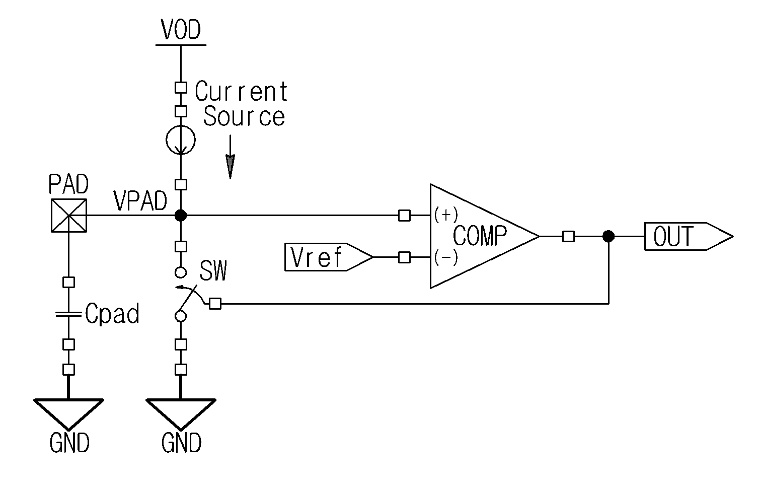
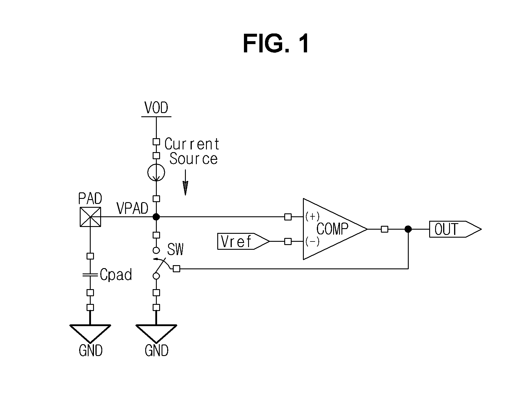
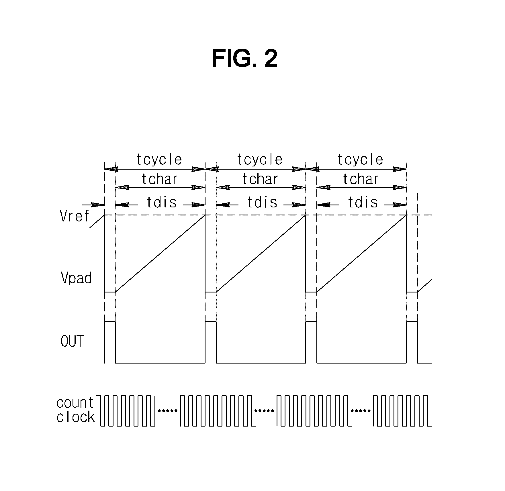
[0041]FIG. 5 is a schematic diagram showing a capacitance measuring circuit for a touch sensor according to the present invention.
[0042]A capacitance measuring circuit for a touch sensor according to the present invention includes a reference voltage generation unit 10 for generating a first reference voltage and a second reference voltage, a MUX unit 60 for selecting one form among electrodes (PAD) 70 when the number of electrodes touched by a user is plural, a comparator 20 for comparing a voltage generated by the reference voltage generation unit 10 with a voltage input from the electrode, a charging/discharging circuit unit 50 for charging the electrode from the first reference voltage to the second reference voltage or discharging the electrode from the second reference voltage to the first reference voltage, a timer 40 for measuring the charging time and discharging time of the charging/discharging circuit unit and outputting corresponding output signals, and a control unit 30 for receiving the output signals of the comparator 20 and an external control signal and controlling the charging/discharging circuit unit and the timer.
[0043]FIG. 6 is a detailed view of the capacitance measuring circuit for a touch sensor according to the present invention.
[0044]The reference voltage generation unit 10 is constructed by connecting three resistors, that is, first to third resistors R0, R1 and R2, in series, and generates a first reference voltage Vref_dn and a second reference voltage Vref_up. One terminal of the first resistor R0 is connected to a power source voltage VDD. The second resistor R1 and the third resistor R2 are connected in series. One terminal of the third resistor is connected to a ground GND. The second reference voltage is generated at a node where the first resistor R0 and the second resistor R1 are connected, and the first reference voltage is generated at a node where the second resistor R1 and the third resistor R2 are connected.
[0045]The reference voltage generation unit 10 is not limited to the above construction at all, and the first reference voltage and the second reference voltage may be supplied from the outside, or may be obtained from components, other than resistors.
[0046]The first reference voltage and the second reference voltage generated by the reference voltage generation unit 10 are compared with an electrode voltage Vpad input from the electrode 70, and then respective output signals odn and oup are output. The reference voltage can be varied by varying the resistance values of the reference voltage generation unit 10.
[0047]The comparison of the first reference voltage and the second reference voltage with the electrode voltages Vpad is performed by the comparator 20. The comparator 20 includes a first comparator COMP121 and a second comparator COMP222. The (−) terminal of the first comparator is connected to the second reference voltage, and the (−) terminal of the second comparator is connected to the first reference voltage. Furthermore, the (+) terminal of each comparator is connected to the electrode voltage Vpad. The functions of the comparator 20 are listed in the following table.
Comparator Condition Output value 1 COMP1 Vref_up > Vpad Oup = Low 2 Vref_up > Vpad Oup = High 3 COMP2 Vref_dn > Vpad Odn = Low 4 Vref_dn > Vpad Odn = High
[0048]The control unit 30 controls the charging/discharging circuit unit 50 and the timer 40 based on the output signals odn and oup, output from the comparator 20, and an external control signal CTL1.
[0049]The timer 40 receives an external control signal CTL3 and a clock I_out from the control unit 30, measures the charging and discharging time of the charging/discharging circuit unit 50 based on capacitance existing in the electrode 70, and outputs corresponding signals OUT.
[0050]FIG. 7 is a detailed view of the charging/discharging circuit unit according to the present invention.
[0051]As shown in FIG. 7, the electrode driver 50 includes a current source 51 for supplying a constant current and a switch unit 52 for selecting charging or discharging. The resistor of the current source 51 is a resistor R for determining the amount of bias current of an NMOS transistor n0. The amount of current flowing between the drain and source GND of the NMOS transistor n0 is determined by the resistance value of the resistor R. An NMOS transistor n1 and a PMOS transistor p0 function to mirror the current of the NMOS transistor n0.
[0052]An NMOS transistor n2 and a PMOS transistor p1 are used to perform the charging or discharging of the capacitance of the electrode voltage Vpad, and function to supply an amount of current equal to that of the NMOS transistor n0, which is determined by the resistor R.
[0053]The current source 51 will be described in greater detail. One terminal of the resistor R is connected to a power source voltage VCC, and the other terminal thereof is connected to the drain terminal of the NMOS transistor n0. The source terminal of the NMOS transistor n0 is connected to a ground terminal GND, and the gate terminal the NMOS transistor n0 is commonly connected to the gate terminal of the NMOS transistor n1. Furthermore, the drain and gate terminals of the NMOS transistor n0 are commonly connected to the gate terminal of the NMOS transistor n2. The source terminal of the NMOS transistor n2 is connected to a ground terminal GND, and the drain terminal of the NMOS transistor n2 is connected to the switch unit 52, which will be described later.
[0054]The drain terminal of the NMOS transistor n1 is connected to the drain terminal of the PMOS transistor p0, and the source terminal of the NMOS transistor n1 is connected to a ground terminal GND. The source terminal of the PMOS transistor p0 is connected to a power source voltage VCC, and the gate terminal of the PMOS transistor p0 is commonly connected to the gate terminal of the PMOS transistor p1. The source terminal of the PMOS transistor p1 is connected to a power source voltage VCC, and the drain terminal of the PMOS transistor p1 is connected to the switch unit 52, which will be described later. Furthermore, the drain and gate terminals of the PMOS transistor p0 are commonly connected to each other.
[0055]Meanwhile, variation in the time constant for the value of capacitance, which varies depending on the area of an electrode provided on the PCB of a relevant application product, can be controlled by controlling charging/discharging voltage values in such a way as to change the resistance value of the resistor R of the current source 51.
[0056]FIG. 8 is a detailed view of the switch unit 52 of the charging/discharging circuit unit according to the present invention. As described above, the switch unit 52 is used to select charging or discharging, and includes analog switches or 2-to-1 analog switches and inverters. The switch unit 52 includes a first switch 52a for selecting charging and a second switch 52b for selecting discharging.
[0057]The output signal ‘oup’ of the first comparator COMP1 is connected to the input terminal of a first inverter inv1, and the output signal ‘odn’ of the second comparator COMP2 is connected to the input terminal of the second inverter inv2.
[0058]In the case of the first switch 52a, the output terminal of the first inverter inv1 is connected to the gate terminal of a PMOS transistor p2. The source terminal of the PMOS transistor p2 is connected to the drain terminal of an NMOS transistor n3, and the drain terminal of the PMOS transistor p2 is connected to the source terminal of the NMOS transistor n3. The input terminal of the first inverter inv1 is connected to the gate terminal of the NMOS transistor n3.
[0059]Furthermore, the source terminal of the PMOS transistor p2 and the drain terminal of the NMOS transistor n3 are connected to the drain terminal of the PMOS transistor p2 of the current source 51.
[0060]In the case of the second switch 52b, the output terminal of the second inverter inv2 is connected to the gate terminal of a PMOS transistor p3. The source terminal of the PMOS transistor p3 is connected to the drain terminal of the NMOS transistor n4, and the drain terminal of the PMOS transistor p3 is connected to the source terminal of the NMOS transistor n4. The input terminal of the first inverter inv2 is connected to the gate terminal of the NMOS transistor n4.
[0061]Meanwhile, the source terminal of the NMOS transistor n4, which is connected to the drain terminal of the PMOS transistor p3, is connected to the drain terminal of the NMOS transistor n4, which is connected to the source terminal of the PMOS transistor p3. The source terminal of the NMOS transistor n4 is connected to the electrode voltage Vpad.
[0062]In the case where capacitance increases in the same electrode due to contact with a human body, compared with an existing capacitance, as shown in FIG. 9, the voltage waveform of Vpad is varied from a waveform C0 to a waveform C1. When one cycle is performed, the difference between the time it takes to perform charging and discharging and the existing time is dt0. When two cycles are performed, the difference between the time it takes to perform charging and discharging and the existing time is dt1. When three cycles are performed, the difference between the time it takes to perform charging and discharging and the existing time is dt2. This time difference has the following relationship in proportion to the number of cycles of charging/discharging:
dt2=dt1+dt0
dt1=dt0*2
[0063]That is, dtN=dt0*N, and N=number of cycles of charging/discharging.
[0064]Accordingly, it can be seen that, as the number of cycles of charging/discharging increases, the time it takes to perform the charging/discharging of increased capacitance, compared to existing capacitance, increases proportionally.
[0065]Therefore, the prior art method requires a very fast clock because the time it takes to perform charging or discharging is measured once using a high-speed timer only in the case of charging or discharging in every charging/discharging cycle. In contrast, the present invention can measure a time difference accumulated during N cycles, so that measurement can be performed using a slow clock corresponding to the increased time, compared to the case where the time difference is measured every time. Accordingly, time measurement can be performed more accurately than that in the case where a high-speed clock is used, as in the prior art. As a result, the capacitance formed in the electrode 70 can be measured more accurately.
[0066]Furthermore, if the capacity of charging and discharging current used in the present invention is increased, the time it takes to perform charging or discharging is reduced and the number of charging/discharging cycles during specific periods t4_c0 and t4_c1 is increased in proportion to the amount of increased current. However, it can be seen that a timer value based on the difference between capacitances C0 and C1 at the time that the charging/discharging cycle is terminated near the periods t4_c0 and t4_c1 is not significantly different from a value that is obtained before the capacity of charging and discharging current is increased.
[0067]Accordingly, it can be seen that, although the charging or discharging current has been increased, a relative difference in the charging/discharging time attributable to the existing capacitances C0 and C1 can be kept relatively uniform in the case where the difference is measured after the number of cycles has been increased in reverse proportion to the shortened cycle time.
[0068]FIG. 12 is a flowchart showing the sequence of the operation of the measurement circuit according to the present invention. The sequence of the operation is described below in detail with reference to FIG. 11. In order to calculate capacitance in the electrode 70, an initial voltage Vpad exists in an open state (high impedance) so as to measure charging time and discharging time at step S10.
[0069]Thereafter, when the external control signal CTL1 enters at step S20, the control unit 30 performs discharging so that ‘odn’ becomes 1 and the voltage Vpad is set to a value less than the voltage Vref_dn at step S30.
[0070]The voltage Vpad is compared with the first reference voltage Vref_dn at step S40. If, as a result of the comparison, the first reference voltage is higher than the voltage Vpad, discharging is performed until the first reference voltage becomes lower than the voltage Vpad. After discharging is completed, charging is performed until the voltage becomes Vref_dn again at step S50. The voltage Vpad is compared with the first reference voltage Vref_dn at step S60. If, as a result of the comparison, the voltage Vpad is lower than the first reference voltage, charging is performed until the voltage Vpad becomes higher than the first reference voltage.
[0071]Thereafter, when the voltage Vpad is equal to the first reference voltage Vref_dn, the timer 40 operates and measures the charging time at step S70. It is determined whether charging to a voltage equal to or higher than the second reference voltage Vref_up has been performed at step S80. If, as a result of the determination, the charging to a voltage equal to or higher than the second reference voltage Vref_up has been performed, the charging is completed and the charging time timer is terminated at step S90.
[0072]After the charging to the second reference voltage Vref_up is completed, discharging is performed and, at the same time, the timer operates and measures the discharging time at step S100. When the discharging is completed, the first reference voltage and the voltage Vpad are compared with each other in order to determine whether the discharging to the first reference voltage is completed at step S110. If, as a result of the comparison, the discharging to a voltage equal to or lower than the first reference voltage is completed, the discharging is completed and the measurement of the discharging time is stopped at step S120.
[0073]Accordingly, charging/discharging are performed N times at step S130. The charging or discharging time is measured, and charging timer values tc1, tc2, tc3, . . . , and ten corresponding to respective charging times, discharging timer values td1, td2, td3, . . . , and tdn corresponding to respective discharging times, and a total timer value ‘ta’ it takes to perform charging and discharging are output at step S140.
[0074]In general, the time ta it takes to perform the charging and discharging of the electrode PAD N times is used as the most important reference value to determine the capacitance of an electrode. However, charging timer values and discharging timer values are additionally output in order to determine whether a human body is actually touched because there is an actual tendency for the charging time and the discharging time to vary from each other due to the external environment. Accordingly, the charging and discharging timer values function to help the logical part of a touch sensor circuit to determine whether an external human body has been touched.
[0075]According to the present invention constructed and operated as described above, the parasitic current in a semiconductor and the current having a value significantly higher than noise caused by the external environment can be used to perform the charging and discharging of an electrode. Accordingly, there are advantages in that the time it takes to perform the charging and discharging of the capacitance of an electrode can be measured more stably and accurately, and thus the value of capacitance of the electrode and the variation in the value can also be measured.
[0076]Although the present invention has been described in connection with the preferred embodiment for illustrating the principle of the present invention, the present invention is not limited to the construction and operation. Those skilled in the art will appreciate that various modifications, additions and substitutions are possible, without departing from the scope and spirit of the invention as disclosed in the accompanying claims. Therefore, it should be construed that the entire changes, modifications and their equivalents fall within the scope of the present invention.