Camera module with molded tape flip chip imager mount and method of manufacture

a technology of camera module and flip chip, which is applied in the field of electronic camera module, can solve the problems of high yield loss, difficult to manufacture ceramic circuit board with a high degree of geometric accuracy, and relatively difficult and expensive manufacturing of ceramic circuit board substrates, etc., and achieve the effect of facilitating the mounting of icds

Inactive Publication Date: 2011-08-11
FLEXTRONICS AP LLC
View PDF13 Cites 87 Cited by
  • Summary
  • Abstract
  • Description
  • Claims
  • Application Information

AI Technical Summary

Benefits of technology

[0014]The present invention overcomes the problems associated with the prior art by providing a simplified camera module design that can withstand high manufacturing temperat...

Problems solved by technology

As one example, ceramic circuit substrates are relatively difficult and expensive to manufacture.
Because of the inherent brittleness of ceramic material, uncontrolled fracture often results in high yield losses.
As another disadvantage, it is difficult to manufacture ceramic circuit boards with a high degree of geometric accuracy because of the inherent warpage associated with ceramics.
That is, raw or “green” ceramic material tends to shrink rather unpredictably during the curing or “firing” process.
This is particularly problematic in the large scale production of ceramic circuit boards because a relatively high percentage of ceramic substrates inevitably experience warpage that is too severe for use and, therefore, have to be discarded.
Of course, the strict quality control practices and high yield losses associated with ceramic circuit substrates contribute to both a ...

Method used


Image

  • Camera module with molded tape flip chip imager mount and method of manufacture
  • Camera module with molded tape flip chip imager mount and method of manufacture
  • Camera module with molded tape flip chip imager mount and method of manufacture

Examples


Embodiment Construction

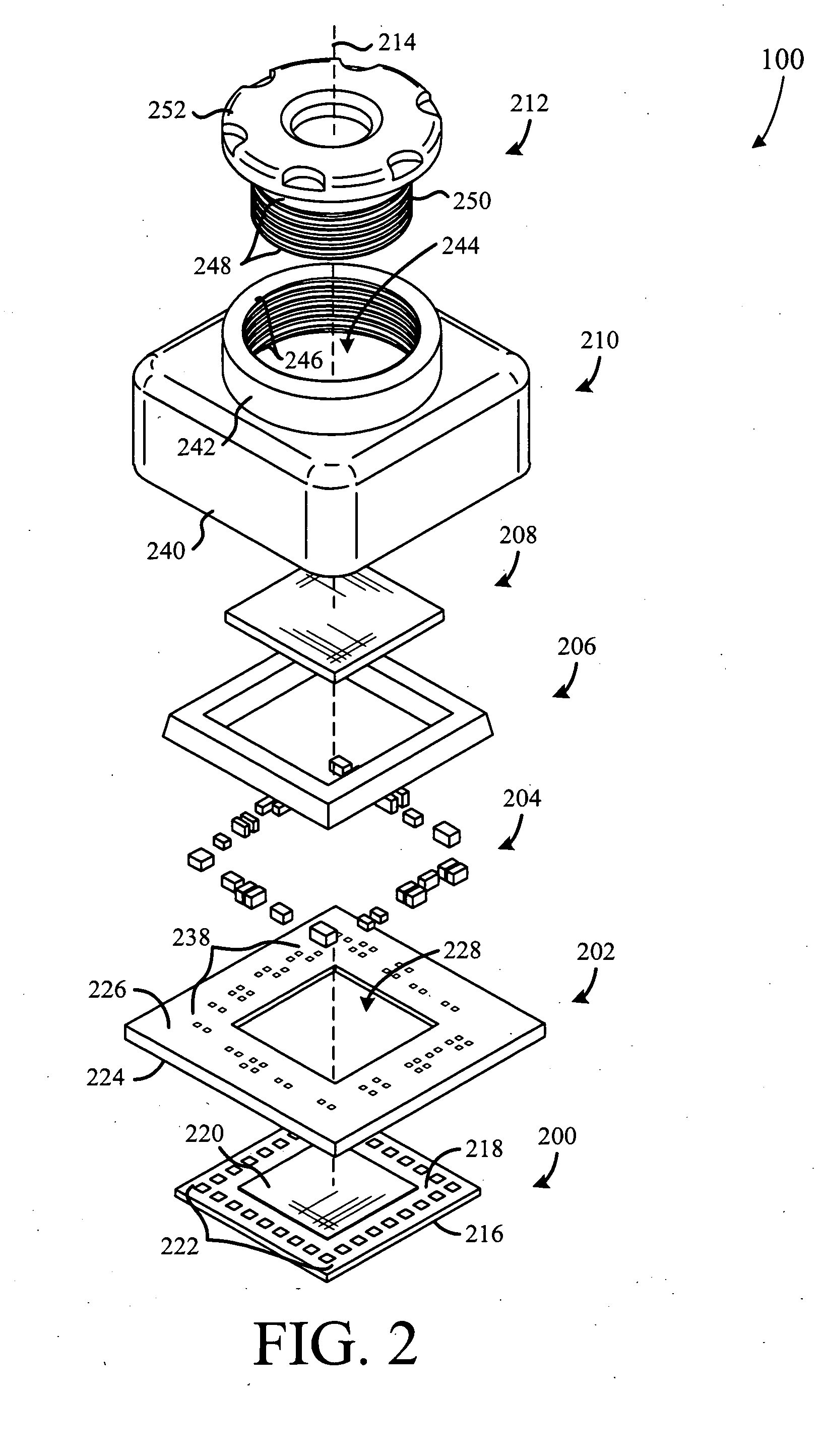
[0050]The present invention overcomes the problems associated with the prior art, by providing a design and method for manufacturing camera modules in a strip format on flexible printed circuit tape. In the following description, numerous specific details are set forth (e.g., number of lenses, adhesives, circuit layout, electrical devices, etc.) in order to provide a thorough understanding of the invention. Those skilled in the art will recognize, however, that the invention may be practiced apart from these specific details. In other instances, details of well known electronic assembly practices and equipment have been omitted, so as not to unnecessarily obscure the present invention.

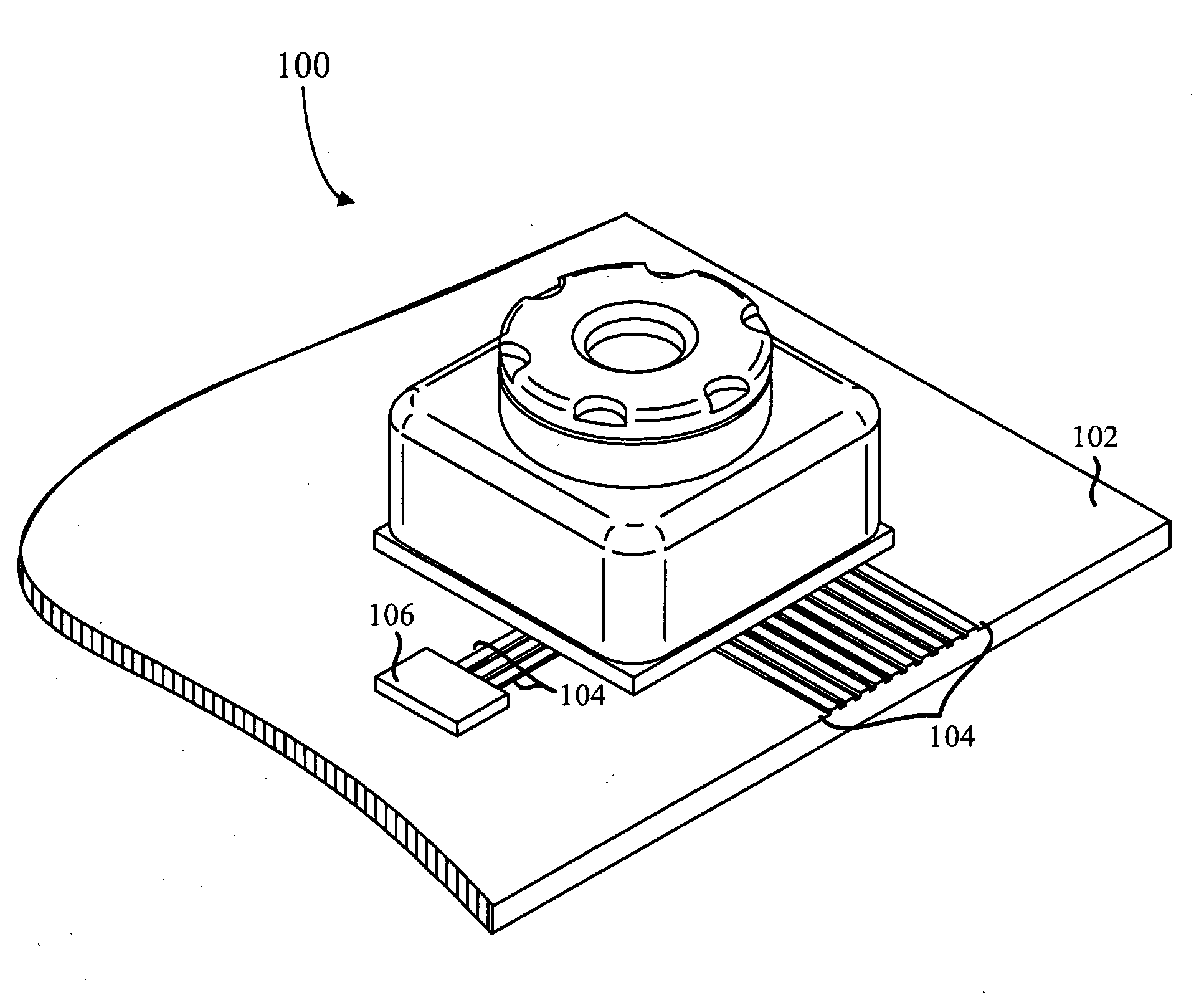
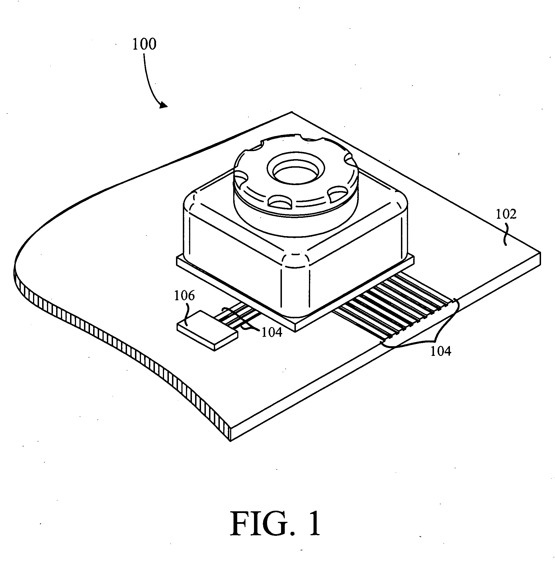
[0051]FIG. 1 is a perspective view of a camera module 100 according to one embodiment of the present invention. Camera module 100 is shown mounted on a portion of a printed circuit board (PCB) 102 that represents a PCB of a camera hosting device. Camera module 100 communicates electronically with other...


PUM


Abstract

A novel design and method for manufacturing camera modules is disclosed. The camera module includes a flexible circuit substrate, an image capture device flip-chip mounted to the bottom surface of the flexible circuit substrate, a housing mounted over the top surface of the flexible circuit substrate, and a lens unit coupled to the housing. In an example embodiment, the camera module includes a stiffener formed directly over a plurality of electrical components mounted on the top surface of the flexible circuit substrate. In another example embodiment, the bottom surface of the flexible circuit substrate defines a recessed portion whereon the image capture device is flip-chip mounted. A disclosed method for manufacturing camera modules includes providing a flexible circuit tape having a plurality of discrete circuit regions, providing a plurality of image capture devices, flip-chip mounting each image capture device on an associate one of the discrete circuit regions, providing a plurality of housings, and mounting each housing on an associate one of the discrete circuit regions.

Description

RELATED APPLICATIONS[0001]This application claims the benefit of priority to co-pending U.S. Provisional Patent Application Ser. No. 61 / 293,842, filed Jan. 11, 2010 by the same inventors and entitled “Camera Module With Molded Tape Flip Chip Imager Mount And Method Of Manufacture,” which is incorporated herein by reference in its entirety.BACKGROUND OF THE INVENTION[0002]1. Field of the Invention[0003]This invention relates generally to electronic camera modules, and more particularly to miniature digital camera modules.[0004]2. Description of the Background Art[0005]Digital camera modules are currently being incorporated into a variety of host devices including, but not limited to, cellular telephones, personal data assistants (PDAs), computers, etc. Therefore, consumer demand for digital camera modules in host devices continues to grow.[0006]Host device manufacturers prefer digital camera modules to be small, so that they can be incorporated into the host device without increasing...

Claims


Application Information

Patent Timeline
IPC IPC(8): H04N5/225
CPCG03B17/02G03B17/12H04N5/2257H04N5/2253H01L27/14618H01L2924/0002H04N23/54H04N23/57H01L2924/00
Inventor TAM, SAMUEL WAISING
Owner FLEXTRONICS AP LLC
Why Eureka
Try Eureka