Wavelength optical filter structure and associated image sensor

a filter structure and wavelength technology, applied in the field of wavelength optical filter structure and image sensor, can solve the problems of inability to eliminate infrared, severe limitation of miniaturisation, and another disadvantag

Inactive Publication Date: 2011-08-25
COMMISSARIAT A LENERGIE ATOMIQUE ET AUX ENERGIES ALTERNATIVES
View PDF8 Cites 40 Cited by
  • Summary
  • Abstract
  • Description
  • Claims
  • Application Information

AI Technical Summary

Problems solved by technology

One important problem to be solved in making an image sensor is to obtain colours.
However, one disadvantage of this sensor is that it cannot eliminate infrared.
This pixel dimension then creates a problem for rays arriving at a high angle of incidence on the sensor surface (edge of image or large objective aperture).
This phenomenon severely limits miniaturisation.
This also is another disadvantage.
There are also absorbing materials other than resins, but although these materials may be more absorbent, they introduce too many manufacturing problems for them to be compatible with the simple production of a matrix of integrated photo-sites, and productio

Method used


Image

  • Wavelength optical filter structure and associated image sensor
  • Wavelength optical filter structure and associated image sensor
  • Wavelength optical filter structure and associated image sensor

Examples


Embodiment Construction

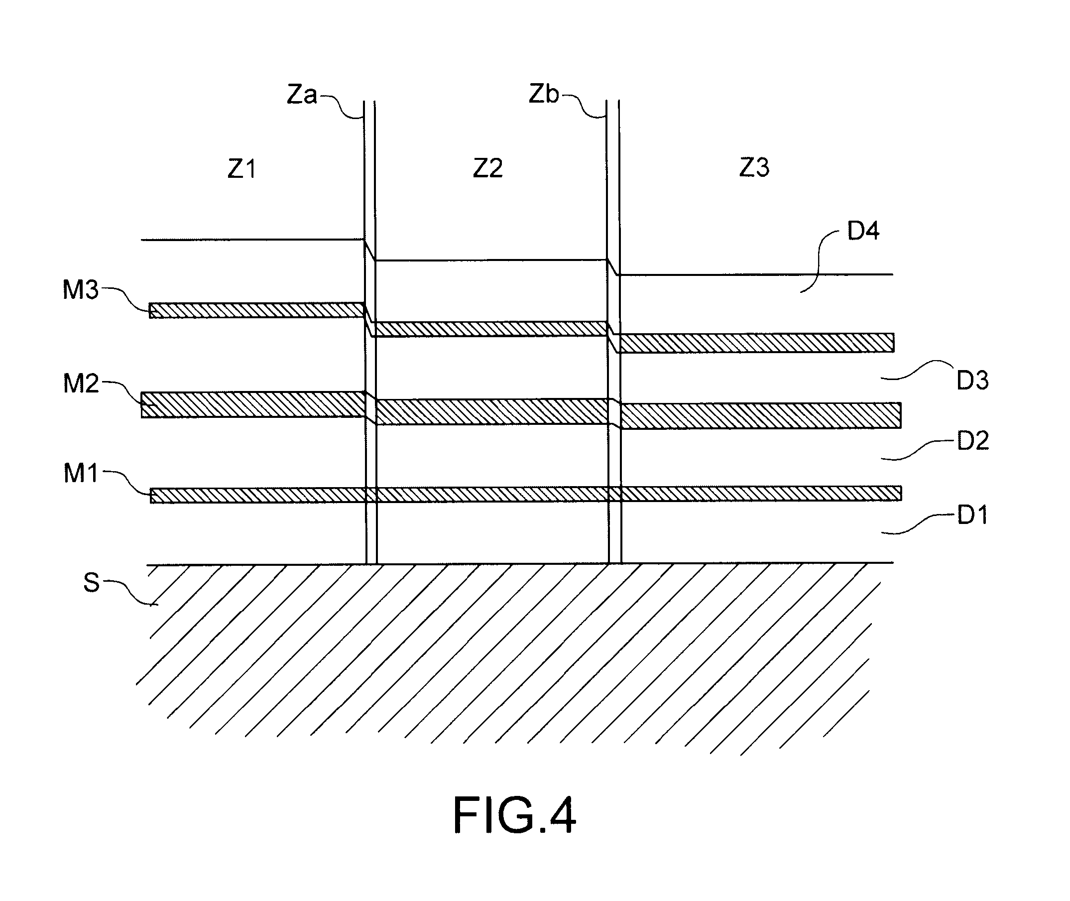
[0056]FIG. 6A shows a sectional view of a first example of an optical filter structure according to the invention.

[0057]The structure in FIG. 6A comprises two dielectric layers d2-d3 and three metallic layers m1-m3 placed on a substrate S. The layers m1, d2, m2 form a first Fabry-Pérot cavity and the layers m2, d3 and m3 form a second Fabry-Pérot cavity. The dielectric layers d2 and d3 are cavity resonators and the metallic layers m1, m2, m3 are mirrors that partially allow light to pass. According to the invention, only the central metallic layer m2 that is common to the two Fabry-Pérot cavities has a variable thickness, the two dielectric layers d2, d3 and the two metallic layers m1, m3 that surround the central layer m2 each have a constant thickness. The structure in FIG. 6A illustrates the embodiment of the invention in which the structure of the stack of dielectric layers and metallic layers is symmetric about the central metallic layer, the dielectric and metallic layers loca...


PUM


Abstract

The invention relates to an optical filter structure composed of at least two adjacent elementary optical filters, an elementary optical filter being centred on an optimum transmission frequency, characterised in that it comprises a stack of n metallic layers (m1-m3) and n−1 dielectric layers (d2-d3), each metallic layer alternating with a dielectric layer such that the central layer in the stack is a metallic layer (m2), each of the layers in the stack having a constant thickness except for the central metallic layer for which the varying thickness fixes the optimum transmission frequency of an elementary filter.

Description

TECHNICAL FIELD AND PRIOR ART[0001]The invention relates to a wavelength optical filter structure and an image sensor that comprises an optical filter structure according to the invention.[0002]The invention has a particularly advantageous application for making small image sensors, for example such as image sensors for miniature cameras in mobile telephones.[0003]The need for image capture by electronic sensors is expanding quickly. The demand for simplified manufacturing of these sensors continues to be very strong. CCD (Charge Coupled Device) sensors are progressively being replaced by CMOS technology-based APS (Active Pixel Sensor) sensors.[0004]One important problem to be solved in making an image sensor is to obtain colours. It is known that most colours can be saved and then reproduced starting from three colours in the visible spectrum (namely red, green and blue).[0005]Some equipment begins by separating the three colours and then guiding them to three image sensors. Other ...

Claims


Application Information

Patent Timeline
IPC IPC(8): H01L31/0232G02B5/22
CPCG02B5/201H01L27/14645H01L27/14621G02B5/288
Inventor GRAND, GILLES
Owner COMMISSARIAT A LENERGIE ATOMIQUE ET AUX ENERGIES ALTERNATIVES
Why Eureka
Try Eureka