Wavelength optical filter structure and associated image sensor
a filter structure and wavelength technology, applied in the field of wavelength optical filter structure and image sensor, can solve the problems of inability to eliminate infrared, severe limitation of miniaturisation, and another disadvantag
- Summary
- Abstract
- Description
- Claims
- Application Information
AI Technical Summary
Benefits of technology
Problems solved by technology
Method used
Image
Examples
Embodiment Construction
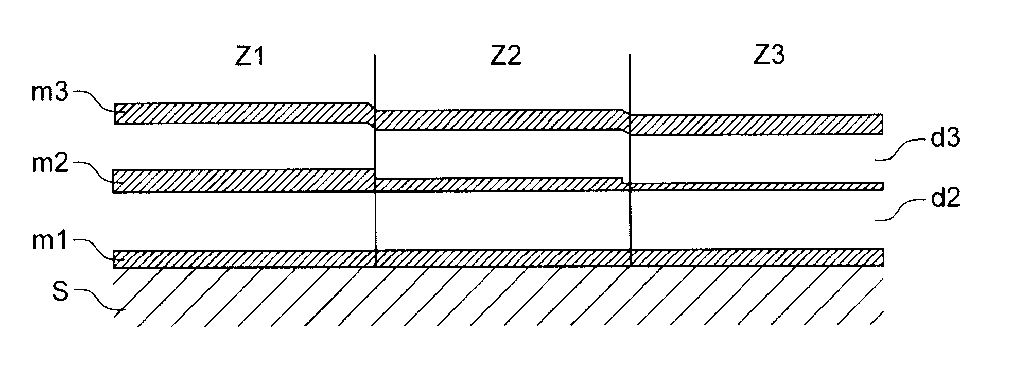
[0057]FIG. 6A shows a sectional view of a first example of an optical filter structure according to the invention.
[0058]The structure in FIG. 6A comprises two dielectric layers d2-d3 and three metallic layers m1-m3 placed on a substrate S. The layers m1, d2, m2 form a first Fabry-Pérot cavity and the layers m2, d3 and m3 form a second Fabry-Pérot cavity. The dielectric layers d2 and d3 are cavity resonators and the metallic layers m1, m2, m3 are mirrors that partially allow light to pass. According to the invention, only the central metallic layer m2 that is common to the two Fabry-Pérot cavities has a variable thickness, the two dielectric layers d2, d3 and the two metallic layers m1, m3 that surround the central layer m2 each have a constant thickness. The structure in FIG. 6A illustrates the embodiment of the invention in which the structure of the stack of dielectric layers and metallic layers is symmetric about the central metallic layer, the dielectric and metallic layers loca...
PUM
 Abstract
Description
Claims
Application Information


