Nonvolatile storage device, access device and nonvolatile storage system

Active Publication Date: 2011-09-15
PANASONIC CORP
View PDF7 Cites 6 Cited by
  • Summary
  • Abstract
  • Description
  • Claims
  • Application Information

AI Technical Summary

Benefits of technology

[0009]An object of this invention is to provide a nonvolatile storage device, an access device and a nonvolatile storage system which have a writing mode for realizing high-speed data writing separate from the writing mode performed against the power shutdown upon performing data writing to the nonvolatile storage device and which can shorten the writing time of contents data upon performing data writing to the nonvolatile storage device.
[0011]According to the foregoing configuration, the writing time of contents data can be shortened by using the second writing mode for realizing high-speed data writing separated from the first writing mode performed against power shutdown upon performing data writing to the nonvolatile storage device.

Problems solved by technology

Nevertheless, when constantly performing data writing which gives consideration to measures during a power shutdown, the processing time required for such data writing which gives consideration to measures during a power shutdown becomes enormous in comparison to the processing time required for data writing that does not give consideration to measures during a power shutdown.

Method used


Image

  • Nonvolatile storage device, access device and nonvolatile storage system
  • Nonvolatile storage device, access device and nonvolatile storage system
  • Nonvolatile storage device, access device and nonvolatile storage system

Examples


Embodiment Construction

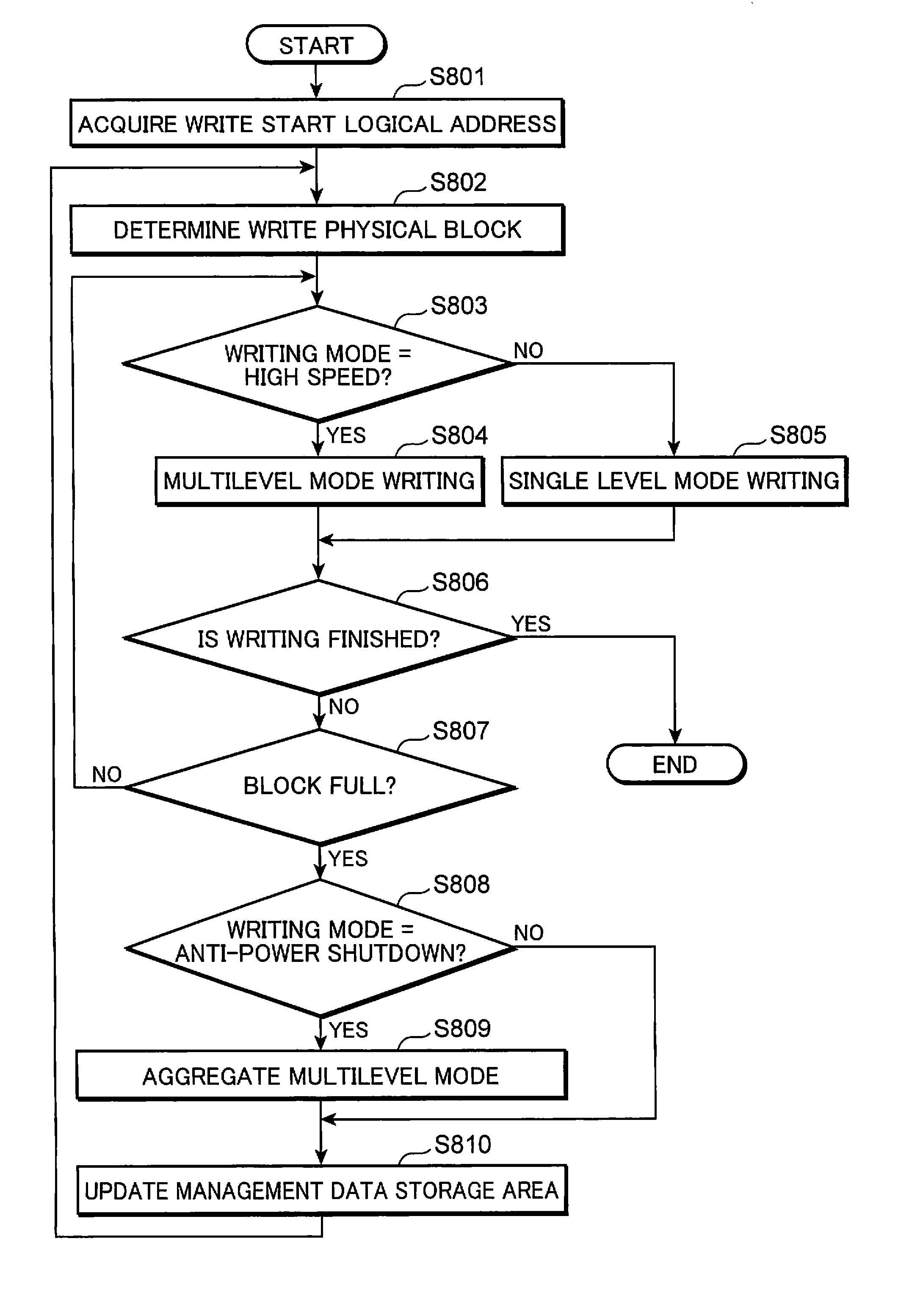
[0022]A nonvolatile memory system according to an embodiment of the present invention is now explained with reference to the appended drawings.

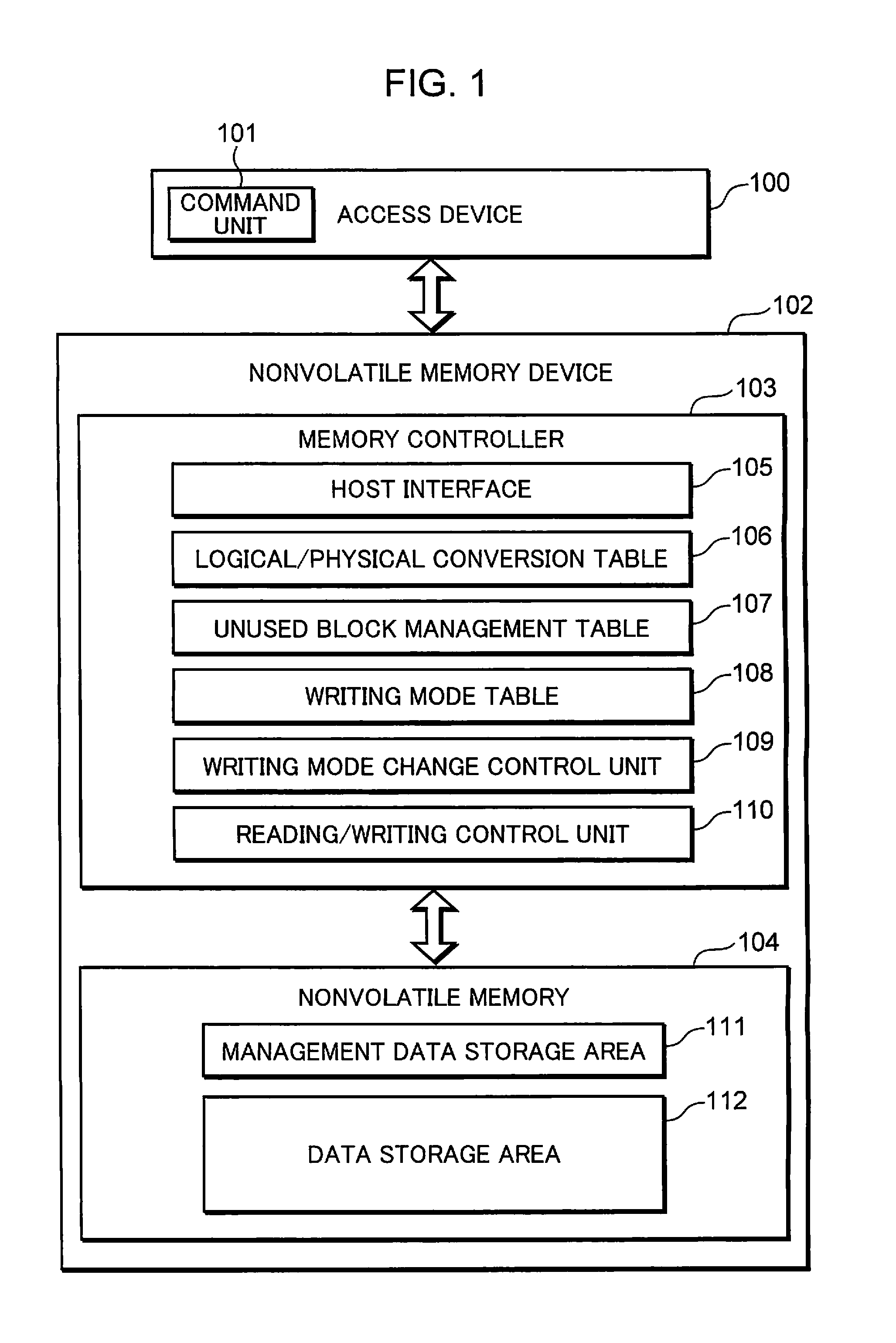
[0023]FIG. 1 is a block diagram showing a configuration of the nonvolatile memory system according to an embodiment of the present invention. The nonvolatile memory system shown in FIG. 1 is an example of a nonvolatile storage system, and includes an access device 100, and a nonvolatile memory device 102. The nonvolatile memory device 102 can communicate with the access device 100, and performs the writing and reading of data according to commands from the access device 100. The nonvolatile memory device 102 is, for example, a semiconductor memory card as an example of a nonvolatile storage device. The access device 100 is a host device that writes and reads data to and from the nonvolatile memory device 102, and is, for example, a digital camera, mobile phone, video recorder, computer or the like.

[0024]The access device 100 comprises a contr...


PUM


Abstract

A memory controller includes a reading / writing control unit for controlling writing and reading of data to and from a physical block of a nonvolatile memory, a writing mode table for storing one of a first writing mode of protecting data against a power shutdown during writing and a second writing mode of writing data at a higher speed than the first writing mode, and a setting unit for setting the writing mode received from an access device in a writing mode table. The reading / writing control unit performs data writing based on the writing mode that has been set in the writing mode table.

Description

BACKGROUND OF THE INVENTION[0001]1. Field of the Invention[0002]The present invention relates to a nonvolatile storage device, an access device for accessing the nonvolatile storage device, and a nonvolatile storage system comprising the foregoing nonvolatile storage device and access device, and in particular relates to a data writing method of the nonvolatile storage device using a nonvolatile semiconductor memory.[0003]2. Description of the Related Art[0004]A semiconductor memory card as a type of medium for recording digital data such as music contents and video contents uses a nonvolatile semiconductor memory such as a flash memory as its storage element.[0005]In recent years, the extended capacity of flash memories is advancing, and high recording density and high data recording speed are becoming required. Moreover, in order to increase the recording capacity of a flash memory, a flash memory capable of recording multiple bits of data in one memory cell (hereinafter referred ...

Claims


Application Information

Patent Timeline
IPC IPC(8): G06F12/00G06F12/02G06F12/16
CPCG06F12/0246G11C11/5628G06F2212/7205G06F11/1446G06F3/0619G06F3/0679G06F3/0652Y02D10/00
Inventor SUTO, MASATOHONDA, TOSHIYUKIMIYATA, KEIZO
Owner PANASONIC CORP
Why Eureka
Try Eureka