High-speed multi-beam parallel laser direct-writing device

A laser direct writing and multi-beam technology, which is applied in photolithographic exposure devices, laser welding equipment, microlithography exposure equipment, etc., can solve the problem of inability to observe the surface of samples, inability to clamp large-scale samples, and inability to achieve high-speed writing and other issues, to achieve the effect of shortening the writing time, improving system reliability, and reducing temperature drift

Active Publication Date: 2011-04-06
安徽中科春谷激光产业技术研究院有限公司
View PDF1 Cites 3 Cited by
  • Summary
  • Abstract
  • Description
  • Claims
  • Application Information

AI Technical Summary

Problems solved by technology

[0004] 1. Using a single beam to write samples point by point, the writing speed is too slow, and it takes too long to write large-scale samples
[0005] 2. Without a microscopic monitoring module, it is impossible to observe the surface of the sample
[0006] 3. The sample to be written is perpendicular to the horizontal plane, which is greatly affected by gravity, and it is impossible to clamp a large range of samples
[0007] 4. With a non-real-time computer as the core controller, the control speed is slow and high-speed writing cannot be achieved

Method used


Image

  • High-speed multi-beam parallel laser direct-writing device
  • High-speed multi-beam parallel laser direct-writing device
  • High-speed multi-beam parallel laser direct-writing device

Examples


no. 1 example

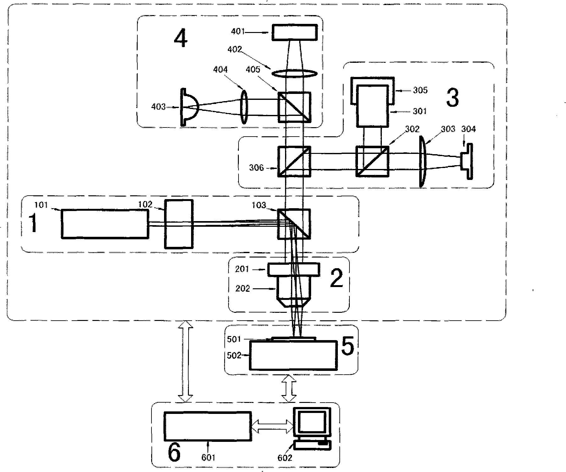
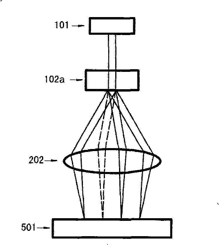
[0057] See first figure 1 , figure 1 It is a schematic diagram of the overall structure of the first embodiment of the high-speed multi-beam parallel laser direct writing device of the present invention, figure 2 This is the basic principle diagram of multi-beam writing in this embodiment. The high-speed multi-beam parallel laser direct writing device of the present invention is composed of six modules: a writing light source modulation module 1, a writing optical head 2, a defocus detection module 3, an illumination and monitoring module 4, a sample stage 5, and a main control module 6.

[0058] The writing light source modulation module 1 includes a laser 101, an acousto-optic modulator 102 and a spectral beam splitter 103. The laser 101 is a gas, solid or semiconductor laser, preferably a semiconductor laser. The spectroscopic beam splitter 102 has high reflectivity for the laser light emitted by the laser 101 and high transmittance for other wavelength laser light. The acou...

no. 2 example

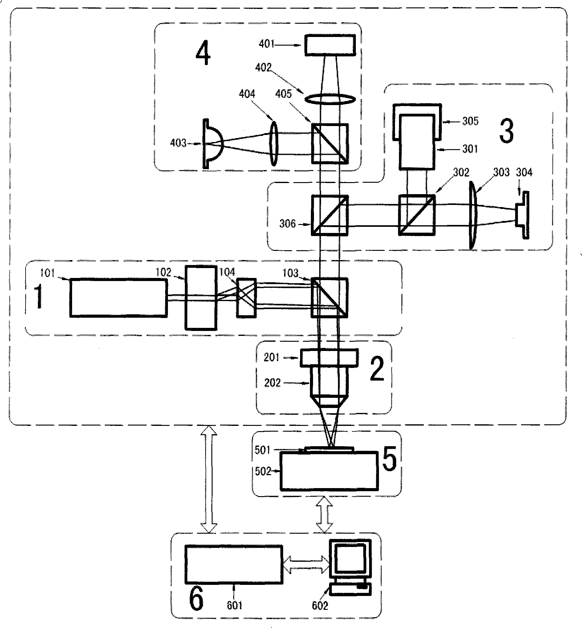
[0086] The overall structure diagram of the second embodiment is as image 3 As shown, its working principle is as follows Figure 4 Shown. Compared with the first embodiment, the feature of this embodiment is that a bi-telecentric lens group 104 is added between the acousto-optic modulator 102 and the spectroscopic beam splitter 103, and the function is to carry out the light beam emitted by the acousto-optic modulator. The beam is expanded and collected at the entrance pupil of the writing objective lens 202, and the beam is filled with the entrance pupil of the writing objective lens 202, thereby having a smaller convergent spot and a smaller size of the writing point.


PUM


Abstract

The invention provides a high-speed multi-beam parallel laser direct-writing device applying to micro-nano processing. The device consists of an inscribing light source modulation module, an inscribing optical header, an out-of-focus detection module, an illuminating and monitoring module, a sample displacement table and a master control module. The device greatly improves inscribing speed by multi-beam laser parallel high-speed inscribing. A multi-beam inscribing sub-system can be combined with sample tables with different motion modes to form inscribing devices with different functions according to the requirement of actual application.

Description

Technical field [0001] The invention relates to the field of micro-nano processing, in particular to a high-speed multi-beam parallel laser direct writing device, which can be applied to micro-electromechanical system (MEMS) device production, semiconductor chip maskless lithography, semiconductor mask production, and binary optics Device manufacturing and other fields. Background technique [0002] In the 21st century, nanotechnology will become one of the driving forces that promote the economic development of countries around the world, and will bring revolutionary changes to industries such as medicine, manufacturing, materials, and information communications. As one of many micro-nano processing methods, laser direct writing technology has many advantages such as low cost, short processing cycle, flexible use, and low environmental requirements. In microelectronics, integrated optics (DOEs), microelectromechanical systems (MEMs), Hybrid integrated circuits and microwave int...

Claims


Application Information

Patent Timeline
Patent Type & Authority Patents(China)
IPC IPC(8): G03F7/00G03F7/20B23K26/06B23K26/08B23K26/42B23K26/064B23K26/70
Inventor 徐文东范永涛
Owner 安徽中科春谷激光产业技术研究院有限公司
Why Eureka
Try Eureka