Antenna element-waveguide converter and radio communication device using the same

a radio communication device and element waveguide technology, applied in waveguide horns, antennas, electrical devices, etc., can solve the problems of insufficient contact, direct impact of antenna gain drop, fragile and light, etc., to avoid stress, improve reliability, and avoid the effect of complicating the manufacturing process

Inactive Publication Date: 2011-09-29
SHARP KK
View PDF5 Cites 28 Cited by
  • Summary
  • Abstract
  • Description
  • Claims
  • Application Information

AI Technical Summary

Benefits of technology

[0015]To solve the above-described problems encountered in the conventional art, an object of the present invention is to provide an antenna-waveguide converter improved in reliability by avoiding a stress due to assembly of a substrate and a waveguide, without complicating the manufacturing process and without increasing the product cost.
[0025]In accordance with the present invention having the above-described structure, arranging surfaces of a plurality of rectangular metal plates provided on a first substrate together with an antenna element with a predetermined gap from an opening of a waveguide prevents contact between the first substrate on which the plurality of rectangular metal plates are provided and the waveguide. This avoids a stress that would be caused by assembly of the first substrate and the waveguide, so that an antenna element-waveguide converter improved in reliability can be achieved.

Problems solved by technology

However, the conventional art having the structure as described above raises the following problems.
Generally, a waveguide is a mass of metal, which is rigid and heavy, whereas a substrate is fragile and light.
Therefore, how to connect these two members having different mechanical strengths has been an important structural issue for ensuring the quality of a high frequency line-waveguide converter.
However, since the thickness of the substrate and the shape of the waveguide vary within a range of dimensional tolerances depending on individual differences, merely physically pressing them one upon the other may cause insufficient contact.
Insufficient contact between the substrate and the waveguide may cause a problem in that a drop in antenna gain is directly affected when, for example, an antenna such as a feed horn is integrally molded with the waveguide.
If the waveguide and the substrate are pressed excessively strongly one upon the other for sufficient contact, then, a stress produced at that time may damage the substrate and components such as ICs mounted on the substrate.
However, such connection disadvantageously complicates the manufacturing process, resulting in higher product cost.

Method used


Image

  • Antenna element-waveguide converter and radio communication device using the same
  • Antenna element-waveguide converter and radio communication device using the same
  • Antenna element-waveguide converter and radio communication device using the same

Examples


first embodiment

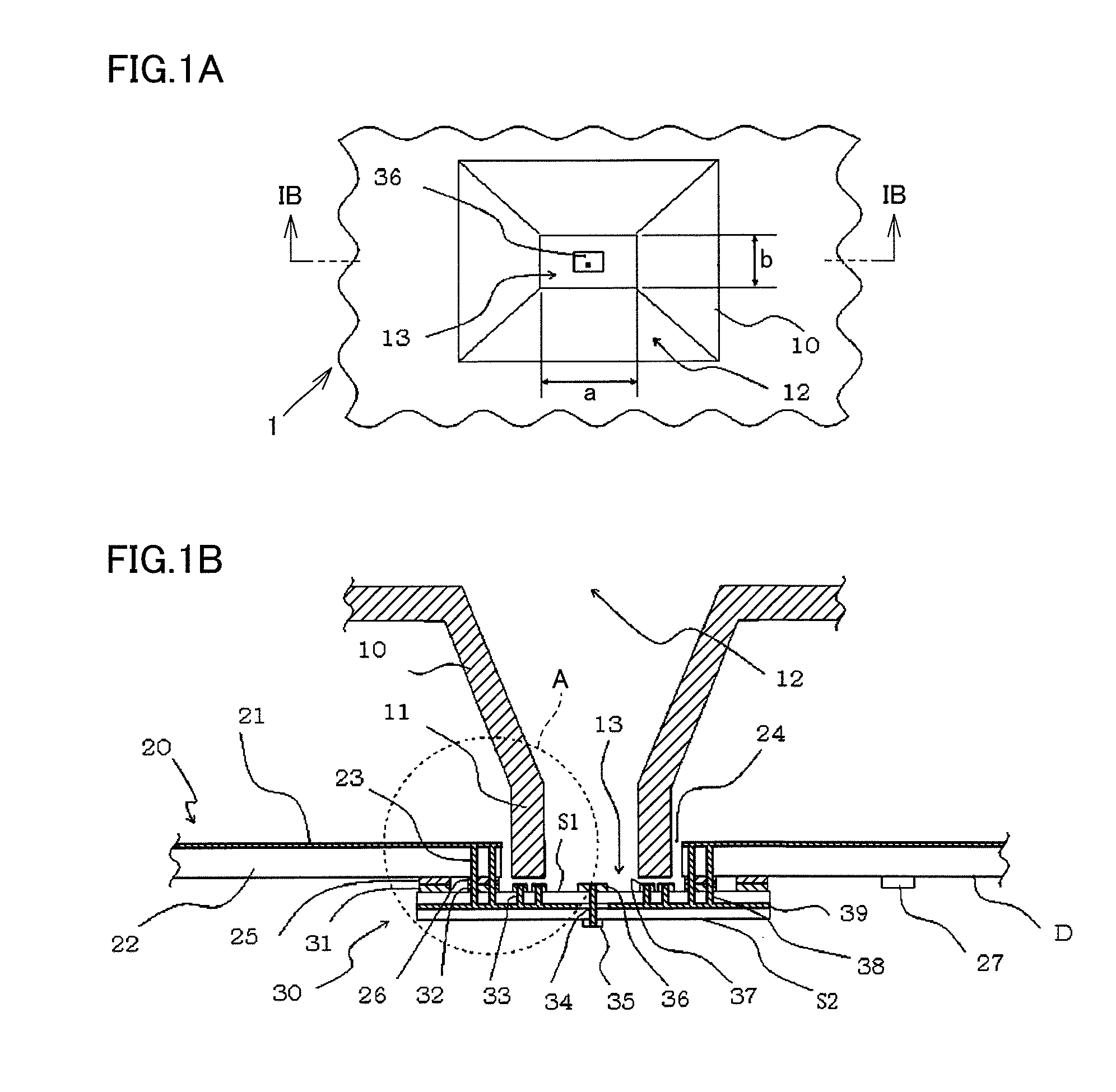
[0034]A first embodiment of an antenna element-waveguide converter of the present invention will be described with reference to FIGS. 1A to 4.

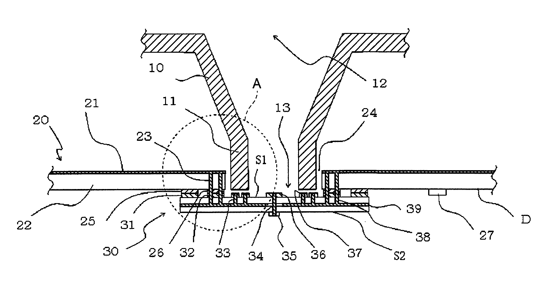
[0035]First, a configuration example of an antenna element-waveguide converter 1 in the first embodiment will be described with reference to FIGS. 1A and 1B. As shown in FIG. 1B, antenna element-waveguide converter 1 includes antenna substrate 30, a waveguide 11 arranged with an opening 13 opposed to a surface of this antenna substrate 30, and horn antenna 10 coupled to waveguide 11. Antenna substrate 30 is mounted on a mounting board 20 in application to a radio communication device. It should be noted that antenna substrate 30, opening 13, and mounting board 20 correspond to a first substrate, a first opening, and a second substrate of the present invention, respectively.

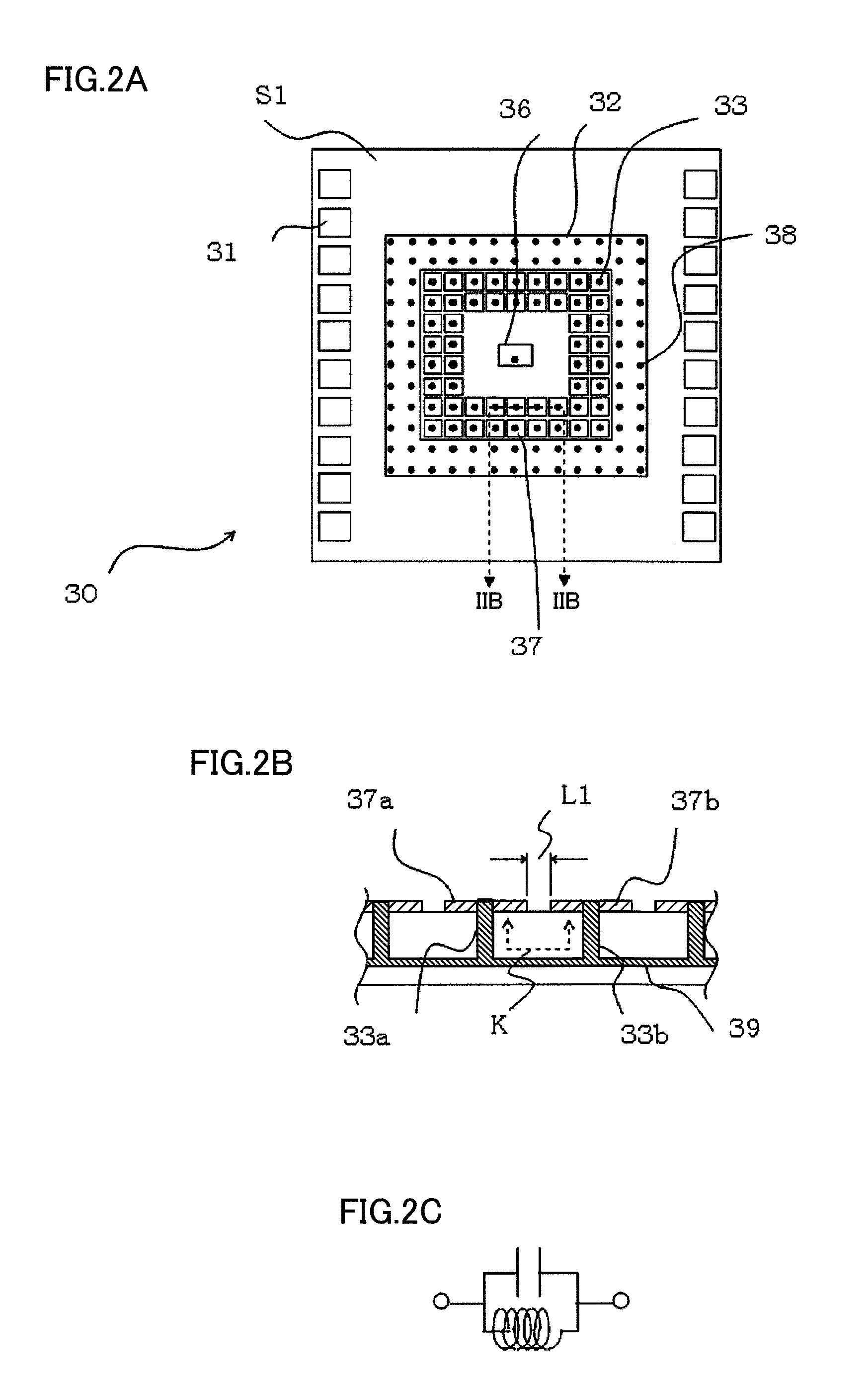
[0036]An example of the overall configuration of antenna substrate 30 will now be described with reference to FIG. 1B. Antenna substrate 30 is implemented by a multilayer su...

second embodiment

[0049]A second embodiment of the present invention will now be described with reference to FIGS. 5A and 5B. Radio communication device 2 is obtained by incorporating antenna element-waveguide converter 1 described in the first embodiment into a housing formed by a chassis 42 and a frame 44, and attaching a signal terminal 43 for connection to an external apparatus (not shown). It should be noted that parts identical to those in the first embodiment are denoted by identical reference characters.

[0050]Chassis 42 and frame 44 are made of resin, and surface mounted component 27, such as a capacitor and a resistor, is mounted in advance on mounting board 20, in addition to antenna substrate 30. Mounting board 20 is attached to chassis 42 at corner portions 45 in the four corners with screws 41. Horn antenna 10 is attached to chassis 42 with screws 40. In more detail, horn antenna 10 and chassis 42 both have L-shaped ends, and are attached to each other with screws 40 after these L-shaped...

third embodiment

[0053]A third embodiment of the present invention will now be described with reference to FIGS. 6A and 6B. FIGS. 6A and 6B show an external appearance of a radio communication device 3. FIG. 6A is a plan view as viewed from horn antenna 10, and FIG. 6B is a cross sectional view taken along the line VIB-VIB in FIG. 6A. Radio communication device 3 is obtained by incorporating antenna element-waveguide converter 1 of the first embodiment shown in FIGS. 1A and 1B into an inner space enclosed by chassis 42 and frame 44, and attaching signal terminal 43 for connection to an external apparatus (not shown), to the outside of a connecting portion of chassis 42 and frame 44. It should be noted that elements in the third embodiment identical to those in the second embodiment are denoted by identical reference characters. The third embodiment differs from the second embodiment in that chassis 42, horn antenna 10, and waveguide 11 are integrally molded of metal, and in that frame 44 is also mad...


PUM


Abstract

An antenna element-waveguide converter includes an antenna substrate having, on one surface, an antenna element and rectangular metal plates arranged in a plurality of rows to surround this antenna element, and a waveguide having, at one end, an opening opposed to the one surface of the antenna substrate. Surfaces of the rectangular metal plates and the opening of the waveguide are arranged with a predetermined gap left therebetween in a direction perpendicular to the one surface of the antenna substrate. Thus arranging the antenna substrate and the waveguide avoids a stress due to assembly variations, which can achieve favorable antenna characteristics.

Description

[0001]This nonprovisional application is based on Japanese Patent Application No. 2010-069513 filed on Mar. 25, 2010 with the Japan Patent Office, the entire contents of which are hereby incorporated by reference.BACKGROUND OF THE INVENTION[0002]1. Field of the Invention[0003]The present invention relates to an antenna element-waveguide converter used for microwave or milliwave band communication, and the radio communication device using the same.[0004]2. Description of the Background Art[0005]In recent years, attention is being focused on radio transmission for a high definition television broadcast (hereinafter referred to as HDTV). Since the HDTV radio transmission involves transmission of a large volume of information, a radio transmission system using milliwaves that can secure a wide transmission bandwidth is being developed. Accordingly, for application to such a radio transmission system, a compact radio communication device is being developed in which a high frequency line ...

Claims


Application Information

Patent Timeline
Patent Type & Authority Applications(United States)
IPC IPC(8): H01Q13/02H01Q13/00
CPCH01Q13/06
Inventor YAMADA, ATSUSHI
Owner SHARP KK
Why Eureka
Try Eureka