
Display panel and display device provided with this

a technology of display panel and display element, which is applied in the field of display panel, can solve problems such as display quality degradation, and achieve the effects of superior designability, reduced display quality degradation, and reduced display quality

Inactive Publication Date: 2011-10-06
SHARP KK
View PDF4 Cites 5 Cited by
  • Summary
  • Abstract
  • Description
  • Claims
  • Application Information

AI Technical Summary

Benefits of technology

[0032]According to the first aspect of the present invention, a peripheral electrode is formed in a picture-frame region on a substrate composing a display panel, in such a way as to cover an electrical wiring line. In addition, peripheral-electrode-giving-potential generating circuit that provides a predetermined potential to the peripheral electrode is provided in the display panel. A potential provided to the peripheral electrode is determined according to a control signal provided to the peripheral-electrode-giving-potential generating circuit from an external source. Hence, for example, a potential can be provided to the peripheral electrode such that the voltage between a second electrode and the peripheral electrode is constant. By this, in a region of the picture-frame region where the peripheral electrode is formed, a constant voltage is applied to a display element during the operation of the display panel. As a result, the occurrence of flicker in the picture-frame region caused by variations in applied voltage to the display element is suppressed.
[0033]According to the second aspect of the present invention, since the peripheral electrode is formed in such a way as to surround a display region, while the outer area of the display region is allowed to have the same color (uniform color), the occurrence of flicker in the picture-frame region can be suppressed.
[0034]According to the third aspect of the present invention, since the peripheral electrode is formed in such a way as to cover all of the electrical wiring line, the occurrence of, flicker in the picture-frame region caused by variations in applied voltage to the display element can be reliably prevented.
[0035]According to the fourth aspect of the present invention, a potential having a predetermined potential difference from a potential of the second electrode, or a potential equal to the potential of the second electrode is provided to the peripheral electrode according to the value of the control signal provided to the peripheral-electrode-giving-potential generating circuit. Hence, by changing the value of the control signal, the magnitude of a voltage applied between the second electrode and the peripheral electrode can be changed. In other words, the color of the picture-frame region can be set to different colors as necessary. By this, a display panel is implemented that is superior in designability to conventional ones, while suppressing the occurrence of flicker in the picture-frame region.
[0036]According to the fifth aspect of the present invention, a potential for black display or a potential for white display is provided to the peripheral electrode according to the value of the control signal provided to the peripheral-electrode-giving-potential generating circuit. Hence, the color of the picture-frame region can be appropriately set to black or white. By this, as with the fourth aspect of the present invention, a display panel is implemented that is superior in designability to conventional ones, while suppressing the occurrence of flicker in the picture-frame region.
[0037]According to the sixth aspect of the present invention, a liquid crystal panel that provides the same effect as that obtained in the first aspect of the present invention is implemented.

Problems solved by technology

In such a liquid crystal panel requiring UV irradiation, if a black matrix is provided in a picture-frame region, then sufficient UV irradiation is not performed in a boundary portion between a display region and the picture-frame region, causing degradation in display quality (e.g., peripheral nonuniformity).

Method used


Image

  • Display panel and display device provided with this
  • Display panel and display device provided with this
  • Display panel and display device provided with this

Examples


Embodiment Construction

[0053]An embodiment of the present invention will be described below with reference to the accompanying drawings.

[0054]

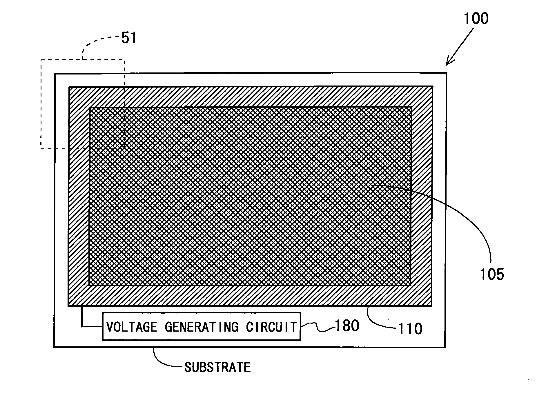
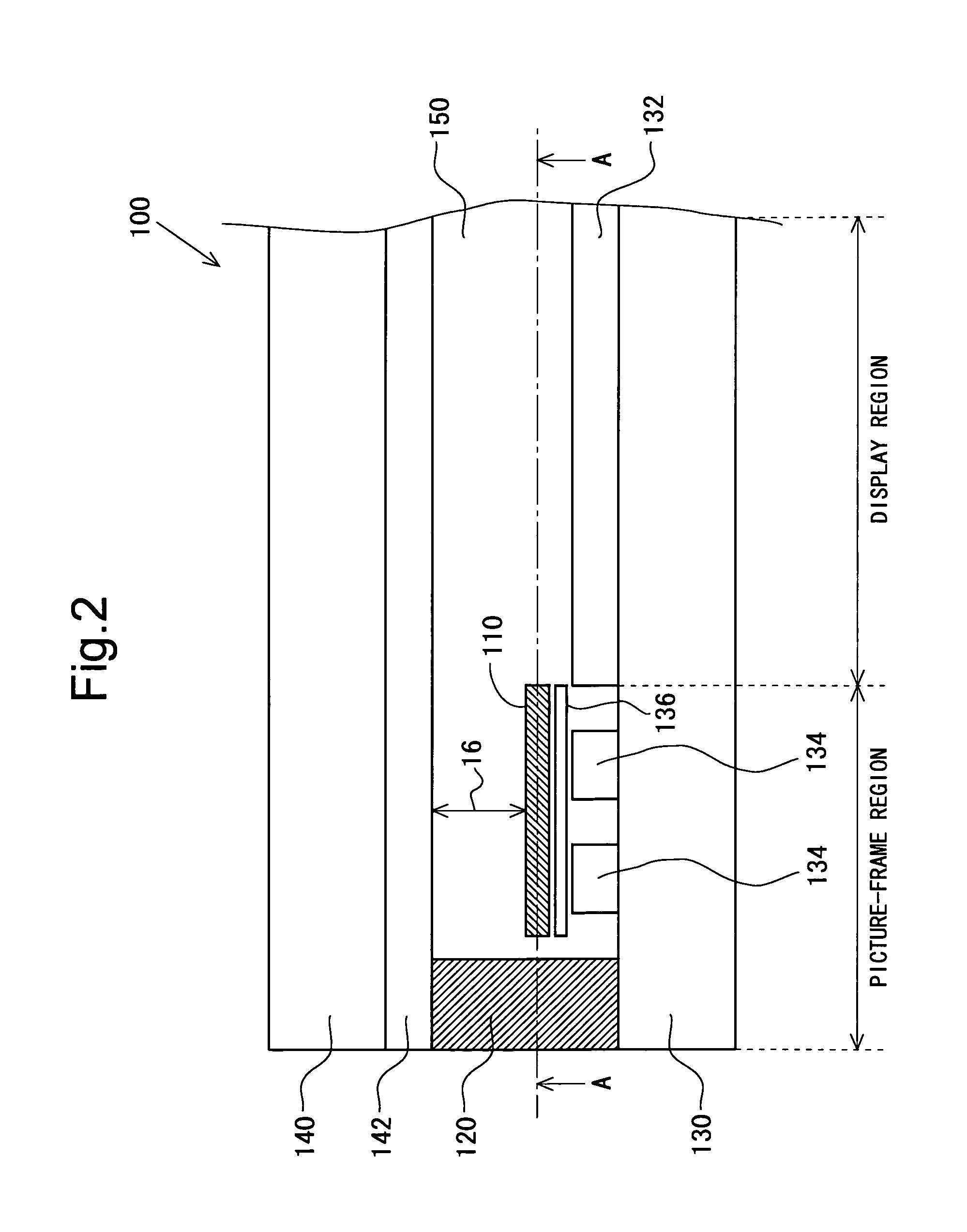
[0055]FIG. 1 is a plan view showing a schematic configuration of a liquid crystal panel 100 according to an embodiment of the present invention. The liquid crystal panel 100 includes a display region 105 which is a region for displaying an image, and a picture-frame region (non-display region) which is a region other than the display region. In the present embodiment, as shown in FIG. 1 in a planar view, in the picture-frame region, an electrode (hereinafter, referred to as the “peripheral electrode”) 110 is formed to surround the display region 105. In addition, a voltage generating circuit 180 for providing a predetermined potential to the peripheral electrode 110 is provided in the picture-frame region of the liquid crystal panel 100. Note that in the following description it is assumed that the display mode of the liquid crystal panel 100 is a normally white mod...


PUM

PropertyMeasurementUnit
voltageaaaaaaaaaa
voltageaaaaaaaaaa
widthaaaaaaaaaa

Abstract

In a display panel having no black matrix in a picture-frame region, occurrence of flicker in the picture-frame region is suppressed. On a substrate constituting a liquid crystal panel, a peripheral electrode is formed in such a way as to cover at least a part of an electrical wiring line arranged in a picture-frame region facing a counter electrode with a liquid crystal layer therebetween. Also, a voltage generating circuit for providing a predetermined potential to the peripheral electrode is provided in the liquid crystal panel. A control signal, which is a binary signal, is provided to the voltage generating circuit from an external source. The voltage generating circuit provides a potential having a predetermined potential difference from a potential provided to the counter electrode, or a potential equal to the potential provided to the counter electrode, to the peripheral electrode according to a value of the control signal.

Description

TECHNICAL FIELD[0001]The present invention relates to a display panel, and more particularly to a technique for suppressing the occurrence of flicker in a display panel having no light-shielding layer in a picture-frame region.BACKGROUND ART[0002]FIG. 9 is a cross-sectional view of a conventional general liquid crystal panel 901. As shown in FIG. 9, the liquid crystal panel901 is composed of a TFT array substrate 930 and a color filter substrate 940 which are a pair of glass substrates. The liquid crystal panel 901 is sectioned into a display region which is a region for displaying an image, and a picture-frame region (non-display region) which is a region other than the display region. In the display region on the TFT array substrate 930 are formed pixel circuits including a TFT array, pixel electrodes 932, and so on. In the picture-frame region on the TFT array substrate 930 are formed electrical wiring lines 934 for driving the pixel circuits. On the other hand, the color filter ...

Claims


Application Information

Patent Timeline
Patent Type & Authority Applications(United States)
IPC IPC(8): G09G5/00
CPCG02F1/1345G02F2001/133388G09G2320/0247G09G3/3611H01L27/3276G02F1/133388H10K59/131
Inventor TAKAHASHI, ISAOYAMAGUCHI, TAKAHIROTAKAHASHI, SHINYAMATSUDA, NOBORU
Owner SHARP KK
Features
  • Generate Ideas
  • Intellectual Property
  • Life Sciences
  • Materials
  • Tech Scout
  • Unparalleled Data Quality
  • Higher Quality Content
  • 60% Fewer Hallucinations
Learn More