Polishing pad and method of use

a technology of polishing pad and surface, applied in the field of polishing pad, can solve the problems of ineffective removal effect and typical surface defects of hard pads

Inactive Publication Date: 2011-10-06
BAJAJ RAJEEV
View PDF10 Cites 0 Cited by
  • Summary
  • Abstract
  • Description
  • Claims
  • Application Information

AI Technical Summary

Benefits of technology

Thus, polishing pads with reduced defectivity, methods of making and using such pads, and materials useful for making same have been described. Although discussed with reference to certain illustrated embodiments, however, the present invention should not be limited thereby and, instead, measured only in terms of the claims, which follow.

Problems solved by technology

Hard pads typically create surface defects such as micro-scratches and are not efficient at effecting the removal of slurry particles.

Method used


Image

  • Polishing pad and method of use
  • Polishing pad and method of use

Examples


Embodiment Construction

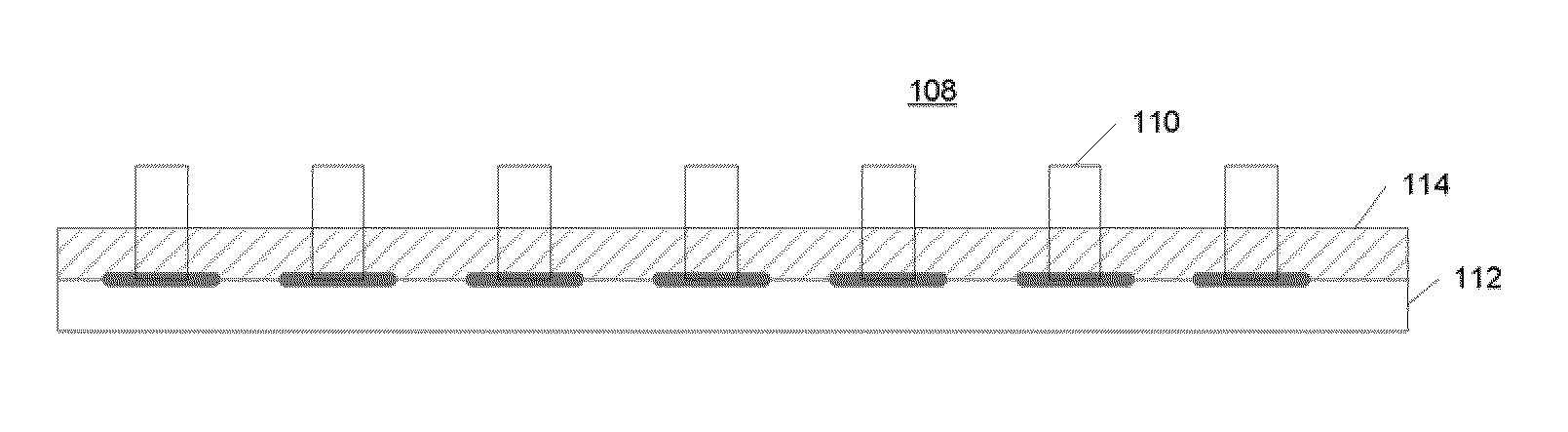
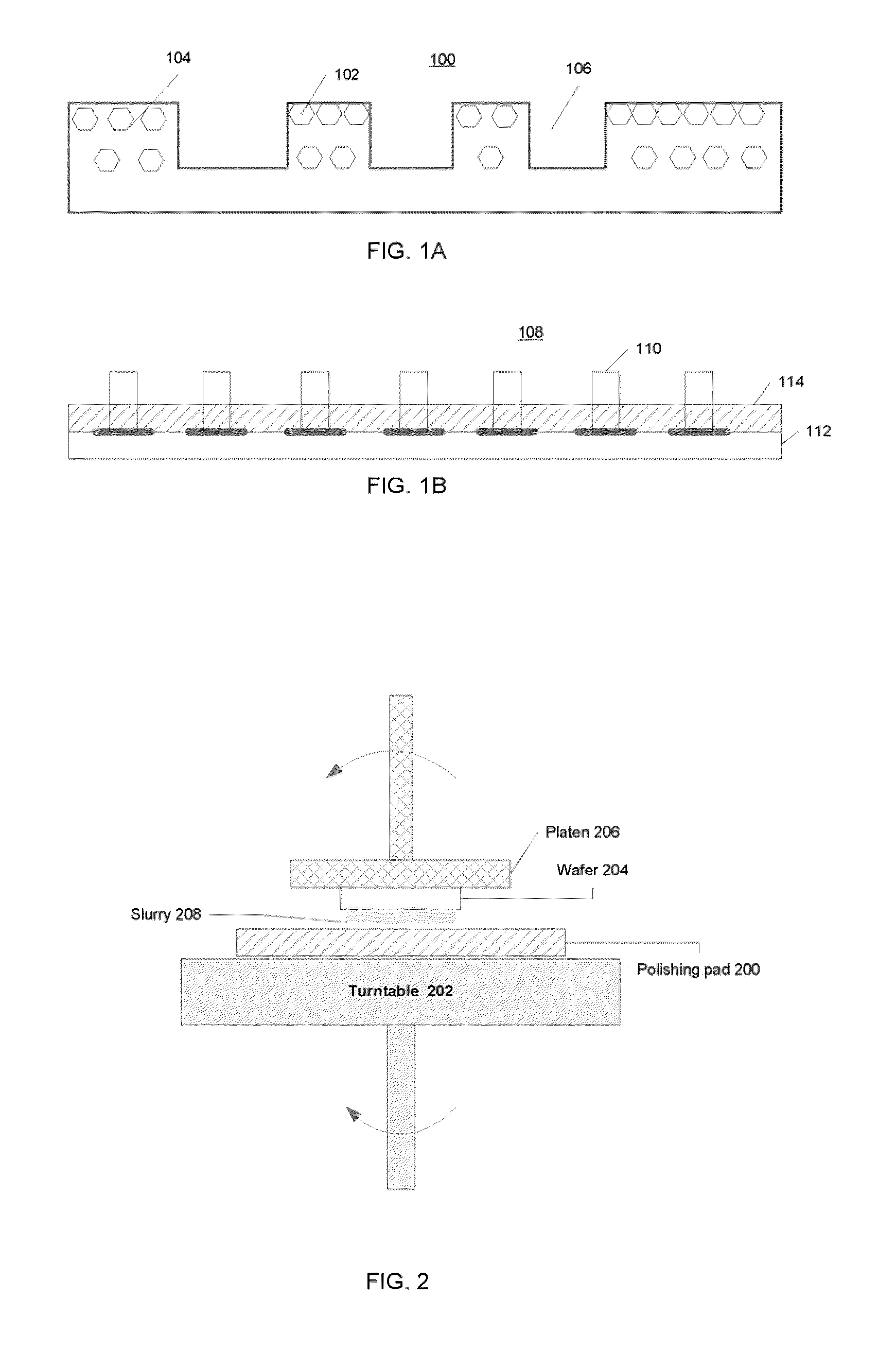
Described herein are a polishing pad with reduced defectivity, methods of using such a pad, and materials useful for making CMP polishing pads with reduced defectivity. As indicated above, CMP involves removing films from the surface of a wafer by pressing a polishing pad against the wafer and rotating these elements relative to one another in the presence of a polishing composition (e.g., a slurry). During the polishing process, a slurry layer forms between the wafer and the pad, thus forming a hydrodynamic boundary layer. Maintaining a uniform fluid layer between the pad and wafer during polishing is important. In cases where the boundary layer is minimized or completely eliminated, the pad may directly contact the wafer leading to a two-body interaction causing higher defectivity. In contrast, a highly lubricated interface will allow more uniform polishing, as well as minimize defectivity. This is particularly important in the case of copper CMP, where the film being polished is ...


PUM

PropertyMeasurementUnit
flexural modulusaaaaaaaaaa
wet Shore D hardnessaaaaaaaaaa

Abstract

A polishing pad has one or more polishing elements made from a hydrogel material having an intrinsic ability to absorb water. The hydrogel material may or may not have micropores, but has a water absorption capability of 4%-60% by weight, a wet tensile strength greater than 1000 psi, a flexural modulus greater than 2000 psi, and a wet Shore D hardness between 25-80, inclusive. The hydrogel material may be made from one or a combination of the following moieties: urethane, alkylene oxides, esters, ethers, acrylic acids, acrylamides, amides, imides, vinylalcohols, vinylacetates, acrylates, methacrylates, sulfones, urethanes, vinylchlorides, etheretherketones, and / or carbonates.

Description

FIELD OF THE INVENTIONThe present invention relates to the field of chemical mechanical planarization (CMP) and, more specifically, to a CMP pad for reduced defectivity.BACKGROUNDIn modern integrated circuit (IC) fabrication, layers of material are applied to embedded structures formed on semiconductor wafers. Chemical mechanical planarization (CMP) is an abrasive process used to remove these layers and polish the surface of a wafer. CMP may be performed on both oxides and metals and generally involves the use of chemical slurries applied in conjunction with a polishing pad that is in motion relative to the wafer (e.g., the pad is often in rotational motion relative to the wafer). The resulting smooth, flat surface is necessary to maintain the photolithographic depth of focus, for subsequent wafer processing steps and to ensure that the metal interconnects are not deformed over contour steps. Damascene processing requires metal, such as tungsten or copper, to be removed from the top...

Claims


Application Information

Patent Timeline
Patent Type & Authority Applications(United States)
IPC IPC(8): B24D11/00B24B37/04
CPCB24B37/042H01L21/32125B24B37/24
Inventor BAJAJ, RAJEEV
Owner BAJAJ RAJEEV
Why Eureka
Try Eureka