Light emitting device

a technology of light emitting device and light emission, which is applied in the direction of semiconductor devices for light sources, discharge tubes luminescnet screens, lighting and heating apparatus, etc. it can solve the problems of difficult to obtain sufficient improvement in both color unevenness and light emission output, and the loss of absorption loss, so as to reduce the probability of light emitted, improve light extraction efficiency, and reduce the effect of absorption loss

Active Publication Date: 2011-10-13
NICHIA CORP
View PDF4 Cites 24 Cited by
  • Summary
  • Abstract
  • Description
  • Claims
  • Application Information

AI Technical Summary

Benefits of technology

[0010]Exposing the side surfaces of the light emitting element from the wavelength converting member allows to decrease the absorption loss due to the wavelength converting member, so that the light extraction efficiency can be improved. Also, this decreases the probability of light emitted from a side surface of the light emitting element being reflected at the wavelength converting member and returning to the light emitting element, which also contributes to improve the light extraction efficiency. On the other hand, together with light propagated through the wavelength converting member, light directly extracted from the exposed side surfaces of the light emitting element to the outside of the wavelength converting member is scattered at the light scattering surface formed at the recess portion, then is extracted as mixed light from the opening at the top plane of the recess portion, so that occurrence of color unevenness can also be suppressed. In the present invention, both the light emitting layer of the light emitting element and the wavelength converting member are spaced apart from the side surface of the recess portion, so that the proportion of light scattered at the light scattering surface formed in the recess portion returning to the light emitting element and / or the wavelength converting member is small. Further, both the light emitting layer of the light emitting element and the wavelength converting member are spaced apart from the side surface of the recess portion, which facilitates light from the light emitting element and the wavelength converting member to be irradiated uniformly on a wider area of the light scattering surface formed in the recess portion, and thus color unevenness can also be satisfactorily suppressed.
[0011]According to the present invention, the light emitting element and the wavelength converting member are spaced apart from the side surface of the recess portion and the side surfaces of the light emitting element are exposed from the wavelength converting member so that light can be directly extracted from the side surfaces of the light emitting element, and a light scattering surface capable of scattering both the light from the light emitting element and the light whose wavelength has been converted by the wavelength converted member is formed on the side surface of the recess portion, and thus the light extraction efficiency can be enhanced while suppressing color unevenness.

Problems solved by technology

However, the reflectance of a silver paste is not sufficiently high and, in addition, a large proportion of the reflected light returns to the light emitting diode chip 8 and is absorbed, resulting in a decrease in the optical output.
However, with such a conventional light emitting device, sufficient improvement in both color unevenness and light emission output has been difficult to obtain.

Method used


Image

  • Light emitting device
  • Light emitting device
  • Light emitting device

Examples


first embodiment

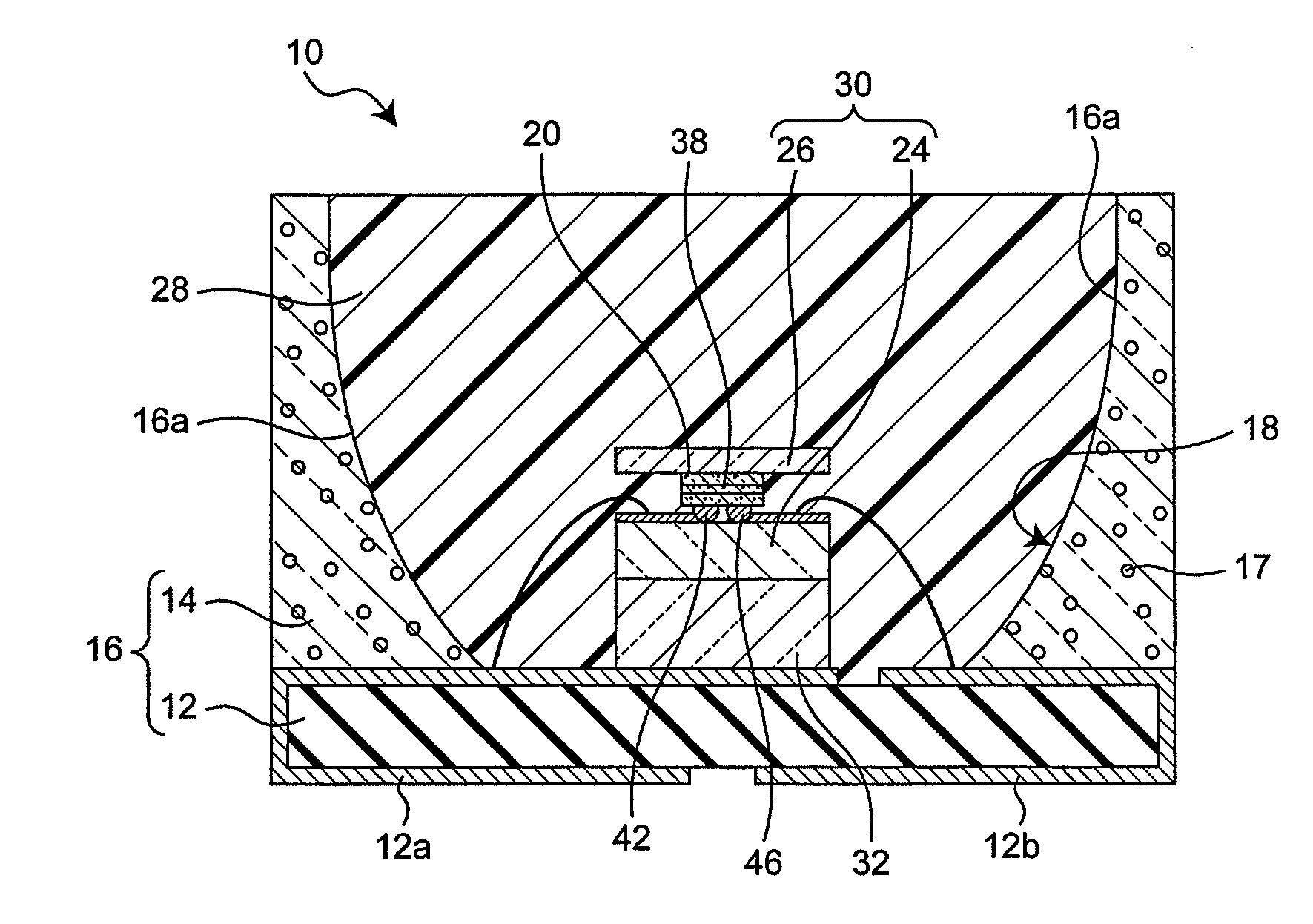
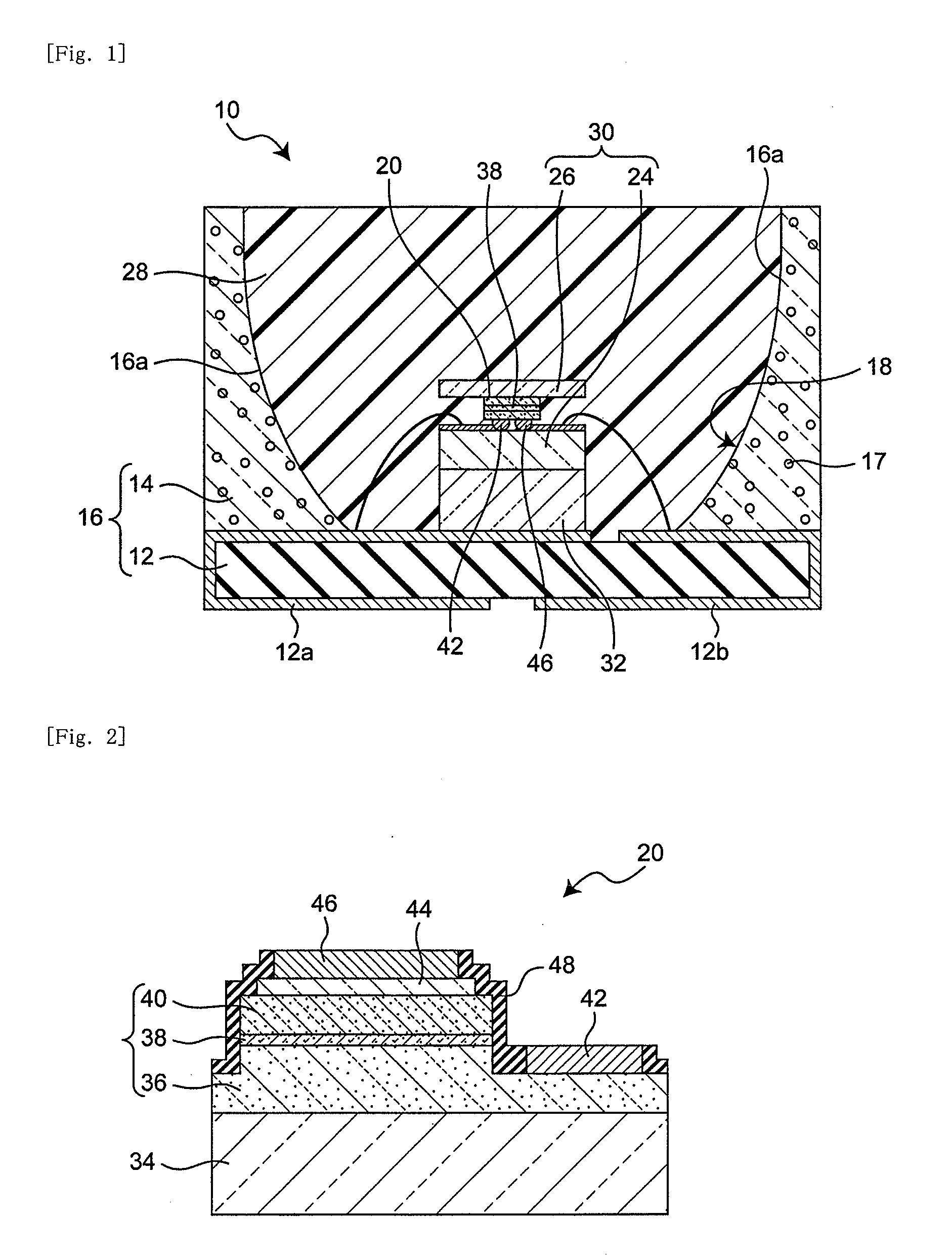
[0025]FIG. 1 is a schematic sectional view showing a light emitting device 10 according to the present invention. A light emitting element 20 and a wavelength converting member 30 for absorbing a part of the light emitted from the light emitting element 20 and converting the wavelength of the light to a different wavelength are housed in a package 16 (housing member). The package 16 of the present embodiment is constructed of a mounting substrate 12 which is a planar insulating member having a wiring formed thereon and an annular side wall 14 formed on the mounting substrate 12. In top view, the package 16 has a rectangular external shape, and a circular cut is performed to form a circular inner side wall 14. The light emitting element 20 has a structure such as shown in FIG. 2, for example, which includes a light emitting layer 38 made of a semiconductor. Further, each of the two electrodes 42, 46 of the light emitting element 20 are connected to the respective wiring 12a, 12b of t...

fourth embodiment

[0101]FIG. 10 is a schematic cross-sectional view showing a light emitting device according to the present invention. In the case of the present embodiment, in the light emitting device 10, the top plane of the recess portion 16a is covered with a light transmissive member 57, and a wavelength converting member 30 capable of absorbing a part of the light emission of the light emitting element 20 and emitting light with a wavelength different than that of absorbed light is fixed at the light emitting element side of the light transmitting member 57. Also, a fluorescent material layer 56 with fluorescent particles 54 dispersed therein is formed on the side surface of the recess portion 16a, where, the fluorescent material particles 54 serve to perform scattering of light emitted from the light emitting element 20 and at the same time also serve to perform wavelength conversion of the light. More specifically, the fluorescent material layer 56, in which the fluorescent material particl...


PUM


Abstract

A light emitting device includes a housing member having a recess open upward, a light emitting element arranged in the recess and having a light emitting layer of a semiconductor, and a wavelength converting member arranged in the recess and capable of absorbing a part of light emission from the light emitting element and emitting light of different wavelength. The light emitting device is capable of mixing the light emission from the light emitting element and the light emission from the wavelength converting member to emit light from the opening of the recess. A light scattering surface for scattering light emission from the light emitting element and wavelength converting member is formed on at least part of the side surface of the recess. The light emitting element and the wavelength converting member are spaced apart from the side and bottom surfaces of the recess, and the side surfaces of the light emitting element are exposed without being covered with the wavelength converting member.

Description

[0001]This application claims priority from Japanese Patent Application Nos. 2010-88331, filed Apr. 7, 2010, and 2010-90250, filed Apr. 9, 2010, the contents of which are incorporated herein by reference in their entireties.BACKGROUND OF THE INVENTION[0002]1. Technical Field[0003]The present invention relates to a light emitting device capable of color-mixing light emitted from a light emitting element and light obtained through wavelength conversion of a part of the original light emitted from the light emitting element, thereby emitting light of a different color.[0004]2. Description of Related Art[0005]A semiconductor light emitting element such as light emitting diode is small in size, has high power efficiency and emits light with clear color. The semiconductor light emitting element also has such advantages as almost free from blowout, excellent startup performance, and high durability to vibration and repetitive operations of turning on and off. There have been developed a li...

Claims


Application Information

Patent Timeline
Patent Type & Authority Applications(United States)
IPC IPC(8): H01J1/62H01J61/40
CPCF21K9/00H01L33/505H01L2224/92247H01L2224/8592H01L2224/73265H01L2224/48257H01L2224/48247H01L2224/48091H01L2224/32245H01L2224/32257H01L2933/0091H01L33/60H01L33/507H01L2924/00014H01L2924/00H01L2924/181H01L2224/16145H01L2924/00012
Inventor ICHIKAWA, MASATSUGU
Owner NICHIA CORP
Why Eureka
Try Eureka