
Light emitting diode

Active Publication Date: 2011-10-20
TSINGHUA UNIV +1
View PDF7 Cites 8 Cited by
  • Summary
  • Abstract
  • Description
  • Claims
  • Application Information

AI Technical Summary

Benefits of technology

[0029]Large-angle light emitting from the second semiconductor layer meets the metal grating to produce a plurality of surface plasmon resonances changing directions of travel of the large-angle light avoiding internal reflection, thus increasing extraction efficiency of the large-angle light. The surface plasmon resonances propagated along surfaces of the metal microstructures can guide and focus the light by a sub-wavelength structure to improve the transmission of the light. Therefore, the extraction efficiency of the large-angle lights can be improved by locating metal grating on the second semiconductor layer. Further, the metal grating can improve the uniformity of the emitted lights of an LED. The metal grating is made of silver because it is a material known for working well in the propagation of the surface plasmons, and so helps improve the extraction efficiency of the LED.

Problems solved by technology

However, extraction efficiency of LEDs is low because typical semiconductor materials have a higher refraction index than that of air.
However, this only affects light having small incidence angles.
Therefore, the large-angle light cannot be efficiently emitted by the LED.

Method used


Image

  • Light emitting diode
  • Light emitting diode
  • Light emitting diode

Examples


Embodiment Construction

[0013]The disclosure is illustrated by way of example and not by way of limitation in the figures of the accompanying drawings in which like references indicate similar elements. It should be noted that references to “an” or “one” embodiment in this disclosure are not necessarily to the same embodiment, and such references mean at least one.

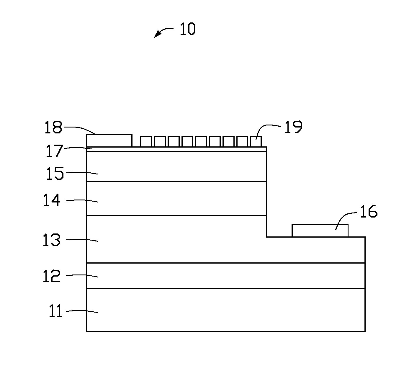
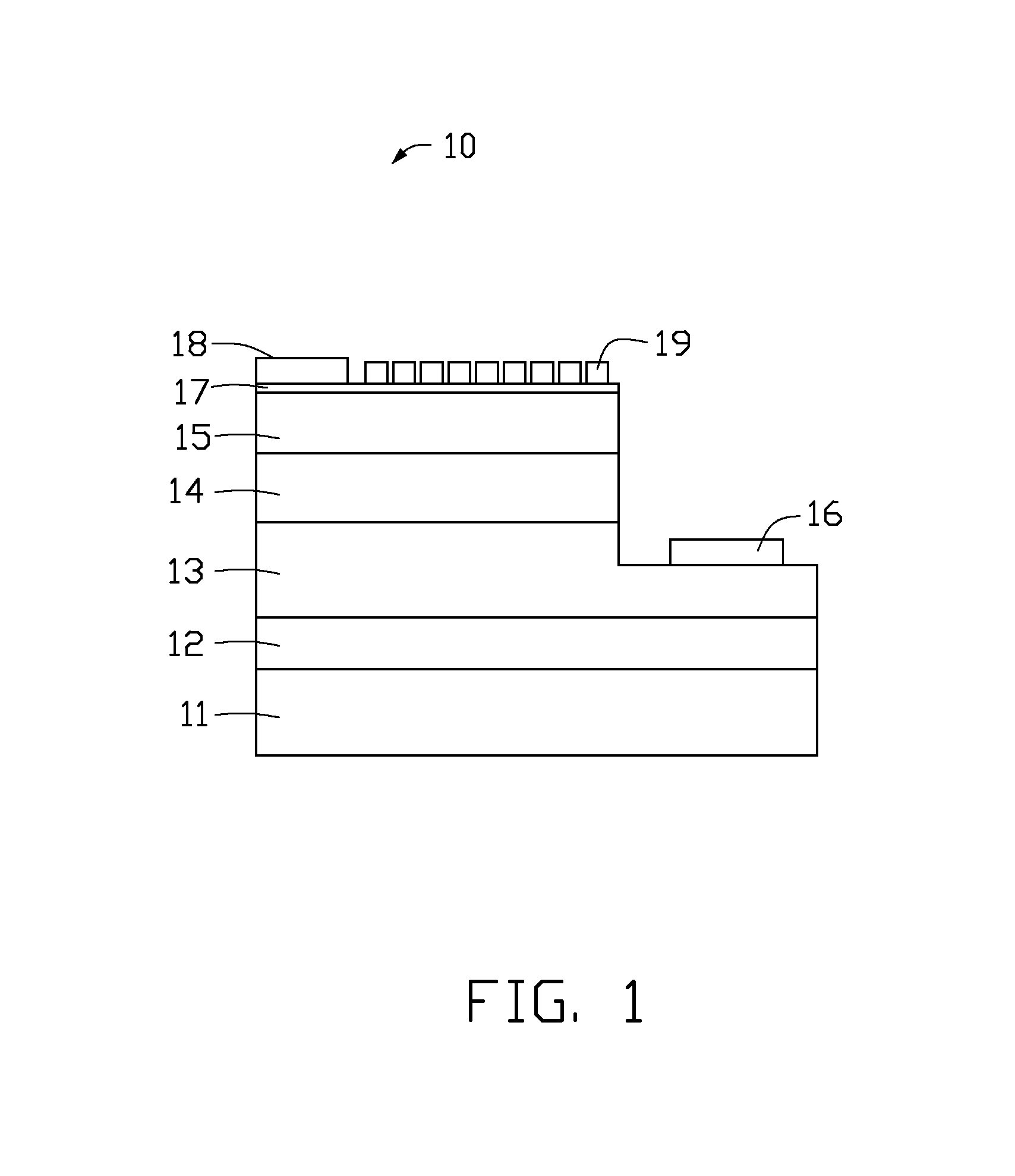
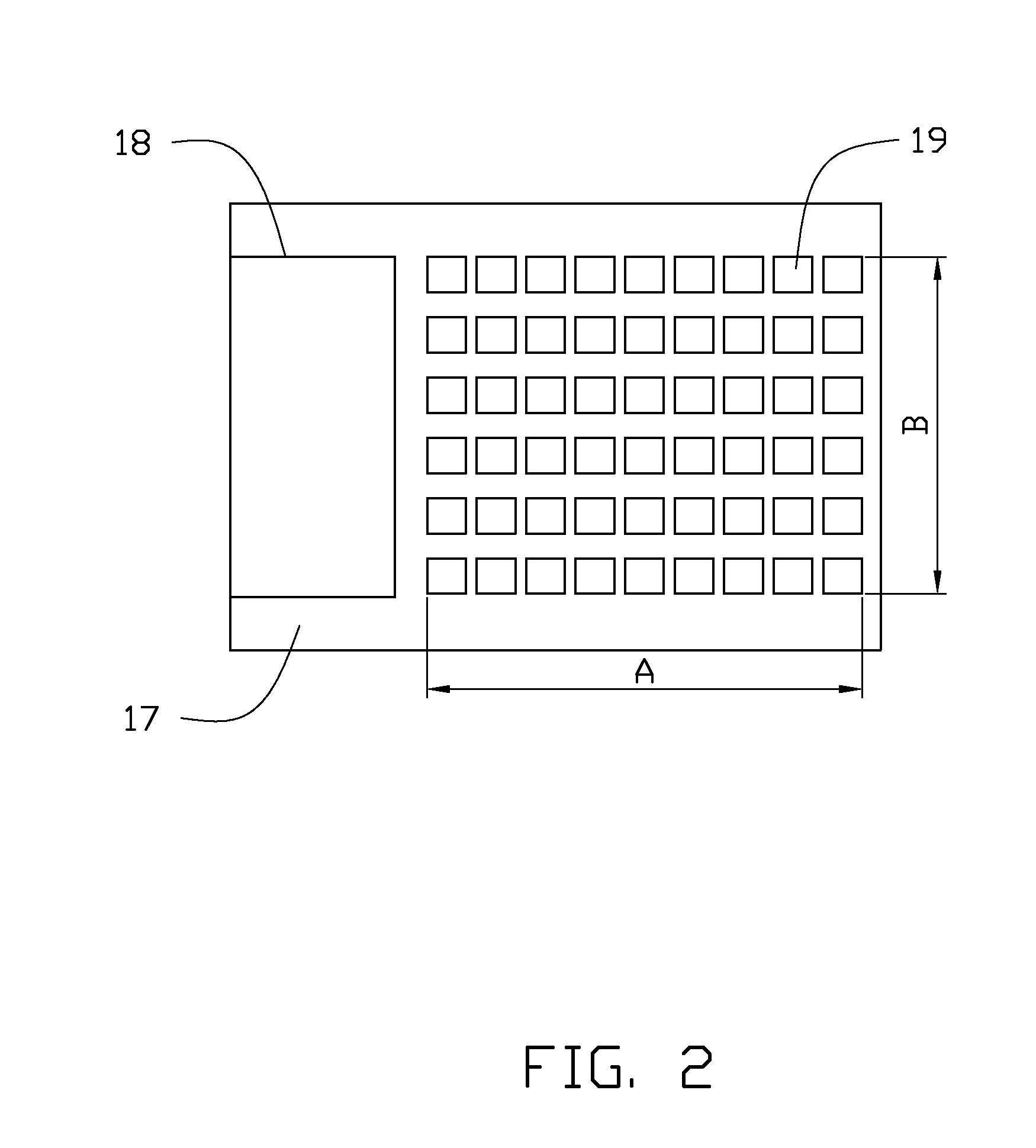
[0014]Referring to FIG. 1, an embodiment of a LED 10 includes a substrate 11, a first semiconductor layer 13, an active layer 14, a second semiconductor layer 15, a first electrode 16, a transparent conductive layer 17, a second electrode 18, and a metal grating 19. The first semiconductor layer 13, the active layer 14, the second semiconductor layer 15 are orderly stacked on the substrate 11. The first electrode 16 is electrically connected to the first semiconductor layer 13. The transparent conductive layer 17 is located on a top surface of the second semiconductor layer 15 away from the substrate 11. The metal grating 19 is located on a top s...


PUM


Abstract

A light emitting diode includes a substrate, a first semiconductor layer, an active layer, a second semiconductor layer, a first electrode, a transparent conductive layer, a second electrode and a metal grating. The first semiconductor layer, the active layer, and the second semiconductor layer are orderly stacked on the substrate. The first electrode is electrically connected to the first semiconductor layer. The transparent conductive layer is located on a surface of the second semiconductor layer away from the substrate. The second electrode is electrically connected to the transparent conductive layer. The metal grating is located on a surface of the transparent conductive layer away from the substrate. The metal grating is a two-dimensional array of a plurality of metal micro-structures.

Description

CROSS-REFERENCE TO RELATED APPLICATIONS[0001]This application claims all benefits accruing under 35 U.S.C. §119 from China Patent Application No. 201010148893.6, filed on Apr. 16, 2010, in the China Intellectual Property Office, the contents of which are hereby incorporated by reference.BACKGROUND[0002]1. Technical Field[0003]The present disclosure relates to a light emitting diode (LED).[0004]2. Description of Related Art[0005]In recent years, highly efficient LEDs made with GaN-based semiconductors have become widely used in different technologies, such as in display devices, large electronic bill boards, street lights, car lights, and other illumination applications. LEDs are environmentally friendly, long working life, and low power consumption.[0006]A conventional LED commonly includes an N-type semiconductor layer, a P-type semiconductor layer, an active layer, an N-type electrode, and a P-type electrode. The active layer is located between the N-type semiconductor layer and t...

Claims


Application Information

Patent Timeline
IPC IPC(8): H01L33/42
CPCH01L33/40H01L33/38
Inventor ZHU, JUNJI, PENGYANG, FENG-LEIJIN, GUO-FAN
Owner TSINGHUA UNIV
Learn More