Schottky Diode with Control Gate for Optimization of the On State Resistance, the Reverse Leakage, and the Reverse Breakdown

a control gate and diode technology, applied in the direction of diodes, semiconductor devices, electrical apparatus, etc., can solve the problems of low reverse breakdown voltage schottky diodes have a relatively high reverse leakage current when compared to conventional pn diodes,

Active Publication Date: 2011-10-20
NAT SEMICON CORP
View PDF1 Cites 6 Cited by
  • Summary
  • Abstract
  • Description
  • Claims
  • Application Information

AI Technical Summary

Benefits of technology

[0034]On the other hand, when a negative voltage is applied to the conductive strips 230 and 232, the top surface of semiconductor material 210 directly below the conductive strips 230 and 232 becomes depleted which, in turn, substantially reduces the reverse leakage current and substantially increases the reverse breakdown voltage. Thus, by selecting the magnitude of the negative voltage, the reverse leakage current and the reverse breakdown voltage can be optimized. As a result, one of the advantages of the present invention is that by biasing the conductive strips 230 and 232 the characteristics of diode 200 can be optimized.
[0035]Another advantage of the present invention is that the present invention eliminates the formation of the p+ guard ring and the contacts along two sides of the anode (e.g., along the two vertical sides of metal region 122 shown in FIG. 1A). By eliminating the formation of the p+ guard ring and the contacts along two sides of the anode, the width of the diode can be reduced which, in turn, increases the frequency of the voltage that can be applied to the anode.

Problems solved by technology

One of the drawbacks of Schottky diodes is that Schottky diodes have a relatively high reverse leakage current when compared to conventional pn diodes.
Another drawback of Schottky diodes is that Schottky diodes have a relatively low reverse breakdown voltage when compared to conventional pn diodes.

Method used


Image

  • Schottky Diode with Control Gate for Optimization of the On State Resistance, the Reverse Leakage, and the Reverse Breakdown
  • Schottky Diode with Control Gate for Optimization of the On State Resistance, the Reverse Leakage, and the Reverse Breakdown
  • Schottky Diode with Control Gate for Optimization of the On State Resistance, the Reverse Leakage, and the Reverse Breakdown

Examples


Embodiment Construction

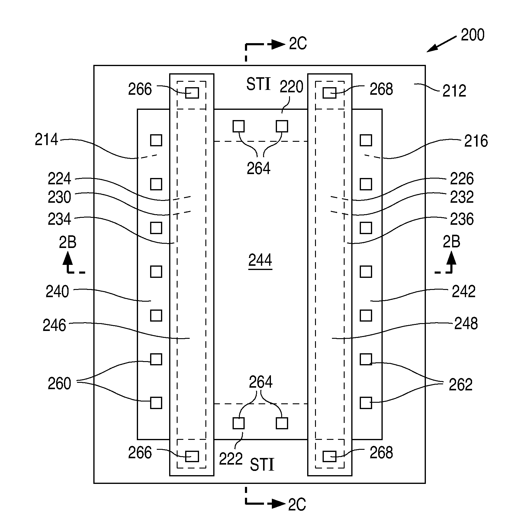
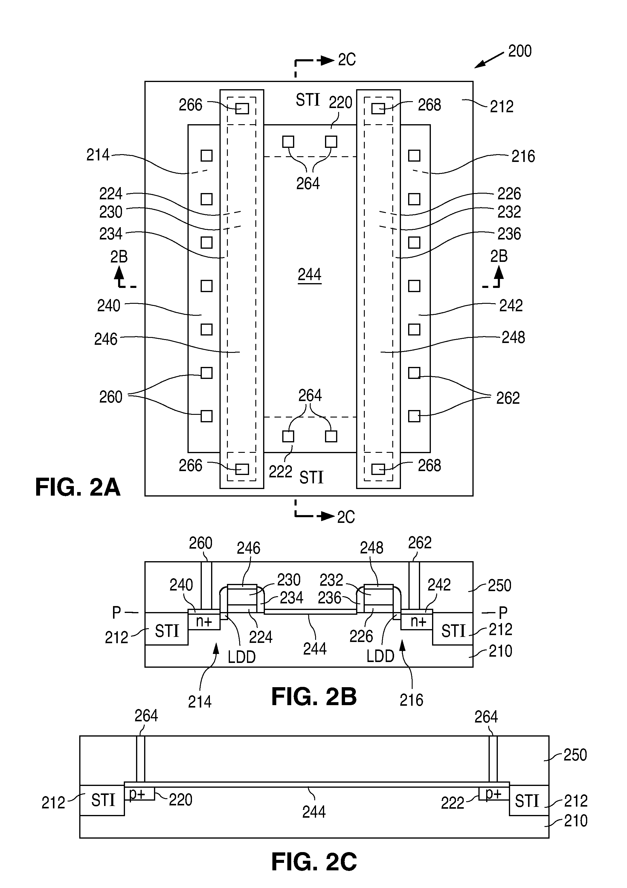
[0020]FIGS. 2A-2C show views that illustrate an example of a Schottky diode 200 in accordance with the present invention. FIG. 2A shows a plan view, FIG. 2B shows a cross-sectional view taken along line 2B-2B of FIG. 2A, and FIG. 2C shows a cross-sectional view taken along line 2C-2C of FIG. 2A.

[0021]As shown in FIGS. 2A-2C, Schottky diode 200 includes an n-type semiconductor material 210, such as an n-type substrate, epitaxial layer, or well, and a shallow trench isolation (STI) ring 212 that is formed in semiconductor material 210. Schottky diode 200 also includes a first n-type strip 214 and a second n-type region 216 that are formed in semiconductor material 210 to touch a portion of the inner side wall of STI ring 212.

[0022]The n-type strips 214 and 216, which each include an n+ region and a low-density drain (LDD) region, are spaced apart and, in the present example, are substantially parallel to each other. As a result, the n-type strips 214 and 216 each has a dopant concentr...


PUM


Abstract

A Schottky diode optimizes the on state resistance, the reverse leakage current, and the reverse breakdown voltage of the Schottky diode by forming an insulated control gate over a region that lies between the metal-silicon junction of the Schottky diode and the n+ cathode contact of the Schottky diode.

Description

BACKGROUND OF THE INVENTION[0001]1. Field of the Invention[0002]The present invention relates to Schottky diodes and, more particularly, to a Schottky diode with a control gate for optimization of the on state resistance, the reverse leakage current, and the reverse breakdown voltage.[0003]2. Description of the Related Art[0004]A Schottky diode is a well-known structure with a metal-to-silicon junction that functions as a diode. Schottky diodes have a forward voltage drop that is lower than the forward voltage drop of a conventional pn diode (e.g., 0.35V versus 0.7V) and a switching action that is faster than the switching action of a conventional pn diode (e.g., 100 ps versus 100 ns).[0005]FIGS. 1A-1C show views that illustrate an example of a conventional Schottky diode 100. FIG. 1A shows a plan view, FIG. 1B shows a cross-sectional view taken along line 1B-1B of FIG. 1A, and FIG. 1C shows a cross-sectional view taken along line 1C-1C of FIG. 1A. As shown in FIGS. 1A-1C, Schottky ...

Claims


Application Information

Patent Timeline
Patent Type & Authority Applications(United States)
IPC IPC(8): H01L29/872H01L21/22H01L21/329
CPCH01L27/0629H01L29/0649H01L29/872H01L29/7835H01L29/0692
Inventor SHAFI, ZIA ALANBABCOCK, JEFFREY A.
Owner NAT SEMICON CORP
Why Eureka
Try Eureka