High frequency power amplifier

a high-frequency power amplifier and amplifier technology, applied in gated amplifiers, amplifiers with semiconductor devices only, amplifiers with semiconductor devices, etc., can solve the problems of insufficient operation efficiency of conventional high-frequency power amplifiers, and achieve wide output power range and improve operation efficiency.

Active Publication Date: 2011-10-27
MURATA MFG CO LTD
View PDF1 Cites 9 Cited by
  • Summary
  • Abstract
  • Description
  • Claims
  • Application Information

AI Technical Summary

Benefits of technology

[0006]In view of the above-described problems, an object of the present invention is to provide a high frequency power amplifier which makes it possible to improve the operating efficiency over a wide output power range.
[0008]The present invention makes it possible to improve the operating efficiency over a wide output power range.

Problems solved by technology

However, conventional high frequency power amplifiers are not good enough to improve operating efficiency when output power is as small as 17 dBm or below.

Method used


Image

  • High frequency power amplifier
  • High frequency power amplifier
  • High frequency power amplifier

Examples


first embodiment

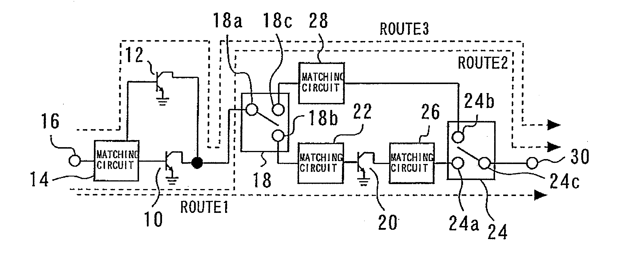
[0025]FIG. 1 is a circuit diagram illustrating a high frequency power amplifier according to a first embodiment. Transistors 10 and 12 are connected parallel to each other and their inputs are connected to a signal input terminal 16 via an input matching circuit 14. The transistors 10 and 12 amplify a high frequency signal inputted from outside to the signal input terminal 16. The input matching circuit 14 matches input impedances of the transistors 10 and 12 to their respective characteristic impedances. The emitter size of the transistor 10 is greater than the emitter size of the transistor 12.

[0026]A switch 18 has an input terminal 18a connected to an output of the transistor 10 and an output of the transistor 12, an output terminal 18b and an output terminal 18c. The switch 18 connects the input terminal 18a to any one of the output terminal 18b and the output terminal 18c.

[0027]An input of a transistor 20 is connected to the output terminal 18b via an inter-stage matching circ...

second embodiment

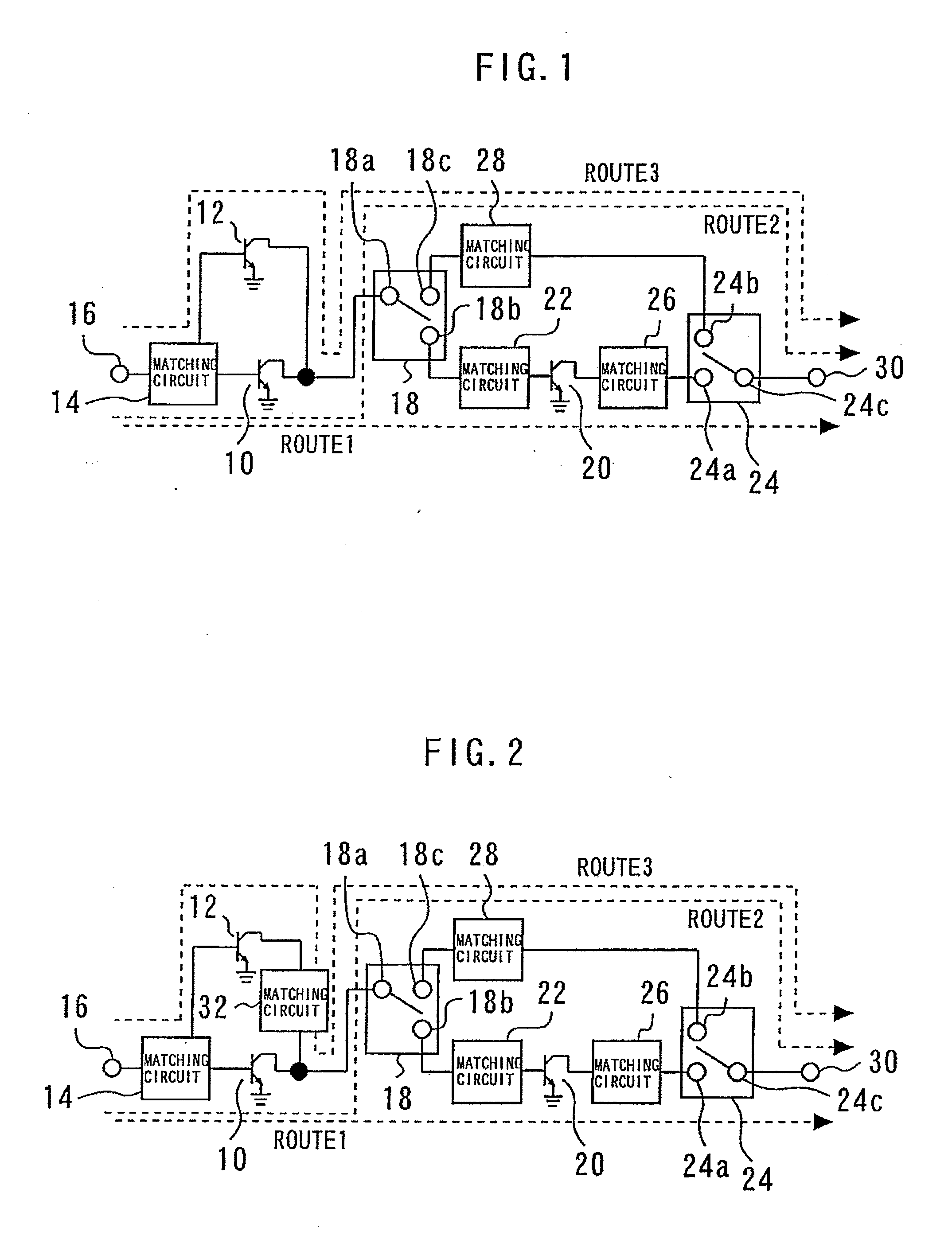
[0034]FIG. 2 is a circuit diagram illustrating a high frequency power amplifier according to a second embodiment. In addition to the configuration of the first embodiment, a matching circuit 32 is connected between a connection point between the output of the transistor 10 and the input terminal 18a, and the output of the transistor 12. The matching circuit 32 matches an output impedance of the transistor 12 with an impedance of the route 3. The matching circuit 32 improves operating efficiency of the transistor 12.

[0035]Table 1 shows operating efficiency of the conventional high frequency power amplifier, the high frequency power amplifier according to the first embodiment and the high frequency power amplifier according to the second embodiment in the case of 7 dBm output. As is understandable from Table 1, the second embodiment can improve operating efficiency compared to the first embodiment.

TABLE 1Operating efficiency in caseof 7 dBm outputConventional high frequency power6%amp...

third embodiment

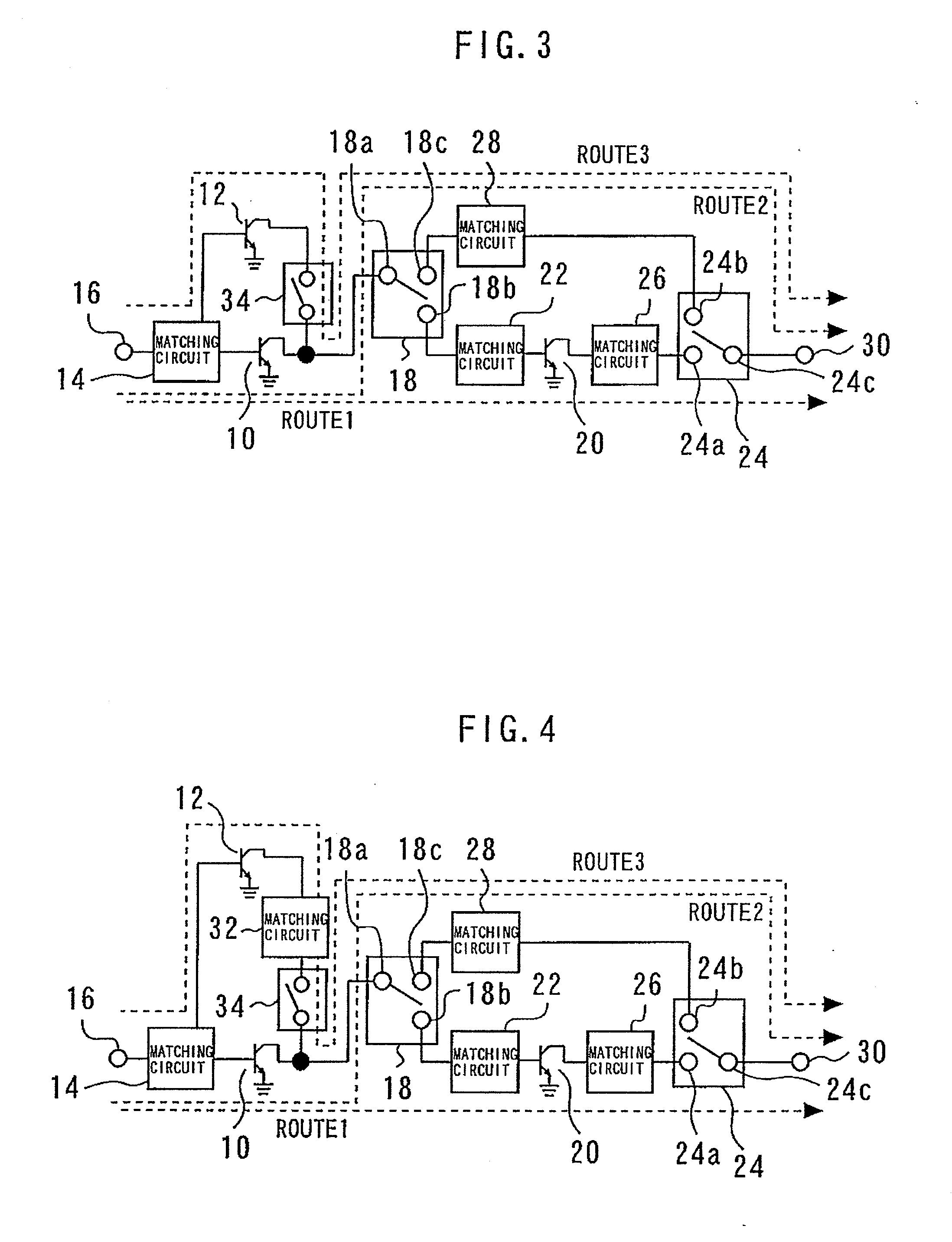
[0036]FIG. 3 is a circuit diagram illustrating a high frequency power amplifier according to a third embodiment. In addition to the configuration of the first embodiment, a switch 34 is connected between a connection point between the output of the transistor 10 and the input terminal 18a, and the output of the transistor 12. When the transistor 10 operates and the transistor 12 does not operate, the switch 34 turns OFF (is left open). The switch 34 can reduce the amount of output power of the transistor 10 leaking to the collector of the transistor 12, and can thereby improve operating efficiency of the transistor 10.

[0037]Table 2 illustrates operating efficiency of the conventional high frequency power amplifier and the high frequency power amplifier according to the third embodiment in the case of 17 dBm output. As is understandable from Table 2, the third embodiment can improve operating efficiency by 3% compared to the conventional art.

TABLE 2Operating efficiency in caseof 17 d...


PUM


Abstract

A high frequency power amplifier includes first and second transistors connected in parallel and amplifying a high frequency signal; a first switch connected to outputs of the first and second transistors and which connects an input terminal selectively to first and second output terminals; a third transistor amplifying a signal output from the first output terminal of the first switch; and a second switch having a first input terminal connected to the third transistor, a second input terminal connected to the second output terminal of the first switch, and which selectively connects the first and the second input terminals to an output terminal of the second switch.

Description

BACKGROUND OF THE INVENTION[0001]1. Field of the Invention[0002]The present invention relates to a high frequency power amplifier which makes it possible to improve the operating efficiency over a wide output power range.[0003]2. Background Art[0004]High frequency power amplifiers that amplify high frequency signals are used for cellular phones and portable terminals. Conventionally, a route in a high frequency power amplifier suitable for large power output operation is used to obtain large power output of 27.5 dBm and a route suitable for medium power output operation is used to obtain medium power output of 17 dBm, and operating efficiency at respective levels of output power is thereby improved (e.g., see Proceedings of the 36th European Microwave Conference, P 348-P 351).SUMMARY OF THE INVENTION[0005]Output power required for a high frequency power amplifier used for a CDMA cellular phone terminal ranges from −50 dBm to 27.5 dBm. However, conventional high frequency power ampli...

Claims


Application Information

Patent Timeline
Patent Type & Authority Applications(United States)
IPC IPC(8): H03F3/217
CPCH03F3/19H03F3/72H03F2203/7239H03F2203/7233H03F2203/7231
Inventor ASADA, TOMOYUKIHARUNA, TAKAOTAKASO, JUN
Owner MURATA MFG CO LTD
Why Eureka
Try Eureka