

Gate driving circuit and display apparatus having the same
a driving circuit and display apparatus technology, applied in the direction of oscillator generators, pulse techniques, instruments, etc., can solve problems such as display defects, and achieve the effect of reducing display defects
- Summary
- Abstract
- Description
- Claims
- Application Information
AI Technical Summary
Benefits of technology
Problems solved by technology
Method used
Image

Examples
embodiment 1
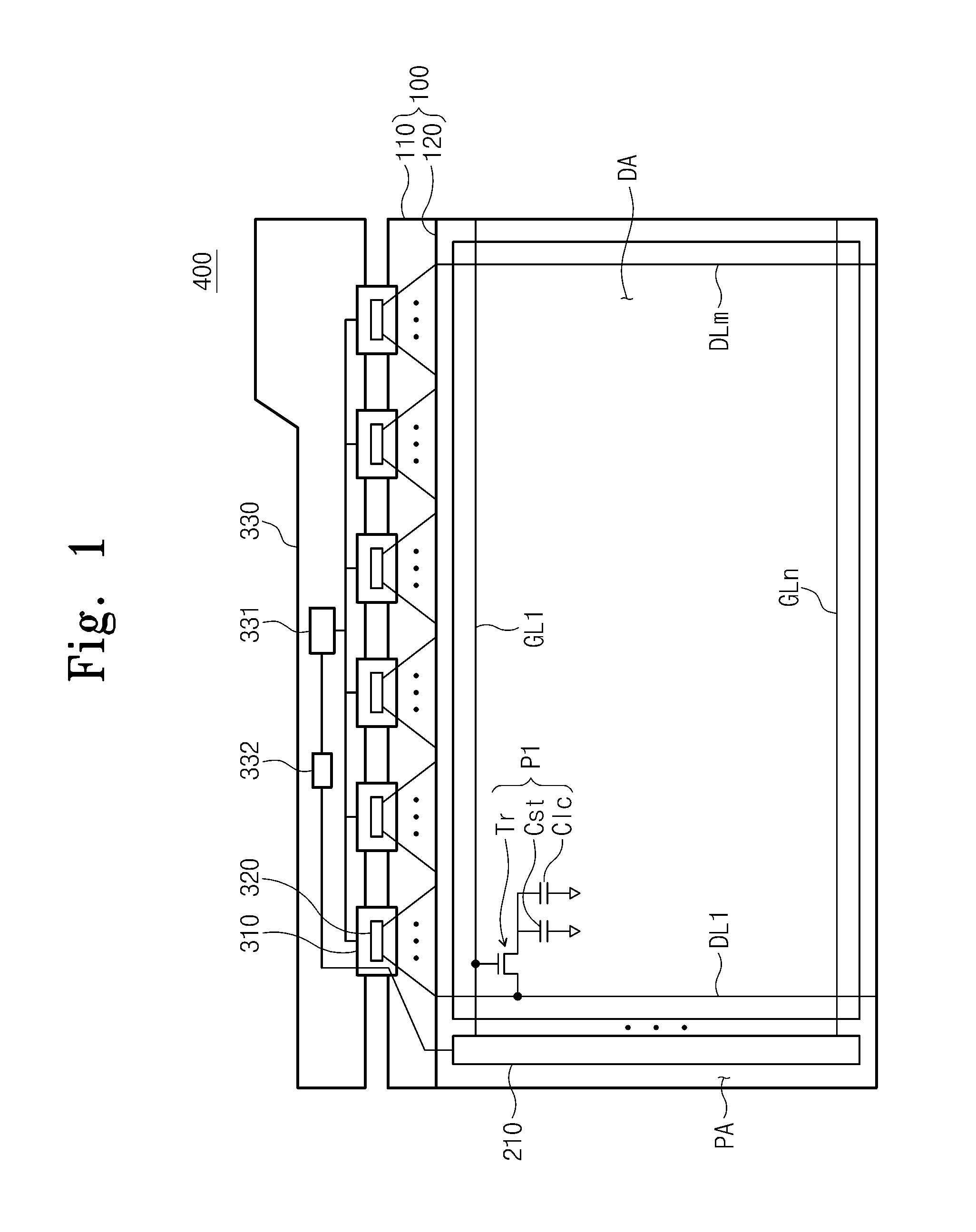
[0037]FIG. 1 is a top plan view showing a first exemplary embodiment of a liquid crystal display (“LCD”) according to the present invention.
[0038]Referring to FIG. 1, an LCD 400 includes an LCD panel 100 displaying an image, a plurality of data drivers 320 outputting a data voltage to the LCD panel 100, and a gate driver 210 outputting a gate voltage to the LCD panel 100.
[0039]The LCD panel 100 includes a lower substrate 110, an upper substrate 120 facing the lower substrate 110, and a liquid crystal layer (not shown) disposed between the lower substrate 110 and the upper substrate 120. The LCD panel 100 includes a display area DA displaying the image and a peripheral area PA adjacent to the display area DA.
[0040]In the display area DA, a plurality of pixel areas is defined in a matrix configuration, and a plurality of gate lines GL1˜GLn and a plurality of data lines DL1˜DLm disposed substantially perpendicular to and insulated from the gate lines GL1˜GLn are arranged on the display...
embodiment 2
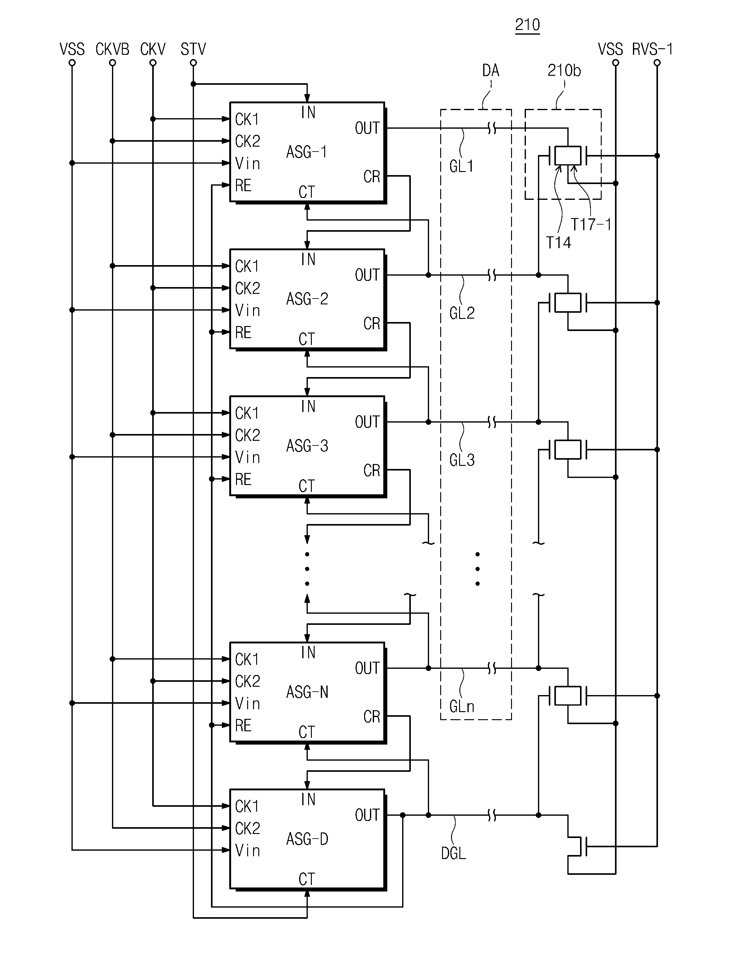
[0084]FIG. 6 is a block diagram showing a second exemplary embodiment of a gate driving circuit according to the present invention, and FIG. 7 is a timing diagram showing first to fourth clock signals and a discharge control signal of FIG. 6. In FIGS. 6 and 7, the same reference numerals denote the same elements in the first exemplary embodiment, and thus the detailed descriptions of the same elements will be omitted.
[0085]Referring to FIGS. 6 and 7, each stage of a gate driving circuit 210 receives two of a first clock signal CK1, a second clock signal CK2, a third clock signal CK3, and a fourth clock signal CK4 to output a gate voltage. In the present exemplary embodiment, odd-numbered stages receive the first clock signal CK1 and the third clock signal CK3, and even-numbered stages receive the second clock signal CK2 and the fourth clock signal CK4. In a first odd-numbered stage ASG-1, the first clock signal CK1 is used as the gate voltage and the third clock signal CK3 is used a...
embodiment 3
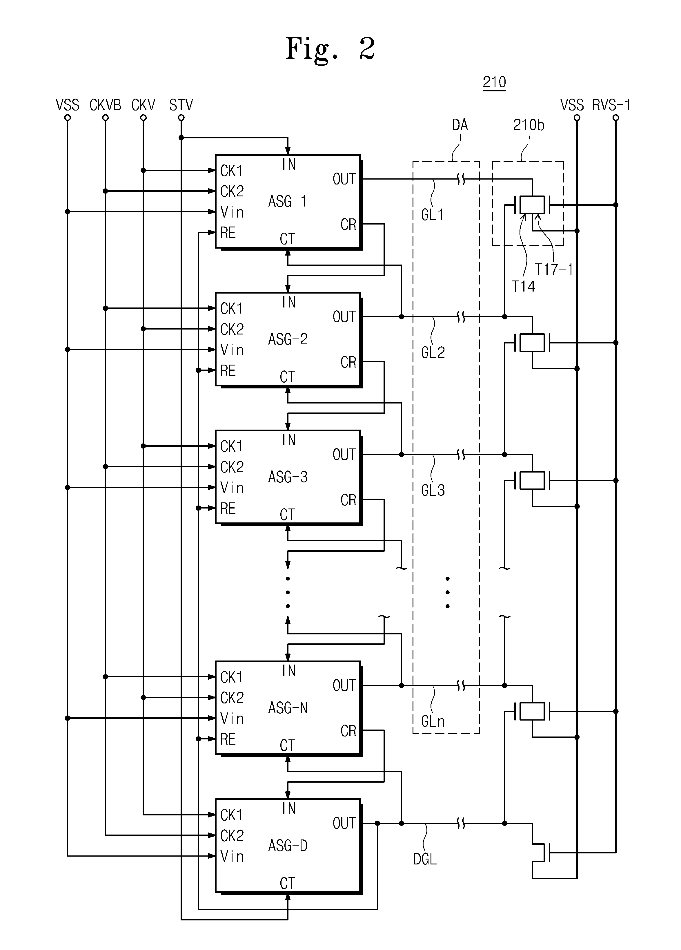
[0092]FIG. 8 is a block diagram showing a third exemplary embodiment of a gate driving circuit according to the present invention. In FIG. 8, the same reference numerals denote the same elements in the first and second exemplary embodiments, and thus the detailed descriptions of the same elements will be omitted.
[0093]Referring to FIG. 8, each stage of a gate driving circuit 210 receives a first clock signal CKV and a second clock signal CKVB to output a gate voltage to a corresponding gate line through the operation of the circuit shown in FIG. 3. In odd-numbered stages, the first clock signal CKV is used as the gate voltage and the second clock signal CKVB is used as a clock signal to prevent the occurrence of the ripple effect. In even-numbered stages, the second clock signal CKVB is used as the gate voltage and the first clock signal CKV is used as the clock signal to prevent the occurrence of the ripple effect.
[0094]A gate control circuit 332 includes a NOR gate circuit 332-1 t...
PUM
 Abstract
Description
Claims
Application Information