
Protection apparatus against electrostatic discharges for an integrated circuit and related integrated circuit

a protection apparatus and integrated circuit technology, applied in emergency protective arrangements for limiting excess voltage/current, emergency protective arrangements for automatic disconnection, amplifiers, etc., can solve the problems of cmos transistor gate oxide, the minimal size of a cmos transistor, and the bipolar and mos transistors are subject to destructive breakdown phenomena

Active Publication Date: 2011-11-03
STMICROELECTRONICS SRL
View PDF4 Cites 12 Cited by
  • Summary
  • Abstract
  • Description
  • Claims
  • Application Information

AI Technical Summary

Benefits of technology

One embodiment is a protection apparatus for protecting against electrostatic discharges for an integrated circuit that is improved with respect to those known.
One embodiment is a protection apparatus against electrostatic discharges for an integrated circuit, said integrated circuit comprising a radiofrequency or higher frequency internal circuit, said internal circuit having a first and a second terminals for the output or the input of a radiofrequency or higher frequency signal, first means for electrically connecting said first and second terminals of the internal circuit to at least a PAD, said integrated circuit comprising at least a first and a second supply circuital lines and at least a first and...

Problems solved by technology

It is known that bipolar and MOS transistors are subject to destructive breakdown phenomena when they undergo overvoltages due to electrostatic charges.
For example, the gate oxide of a CMOS transistor, because of its minimal size, is susceptible to breakdown due to the static electricity, which is commonly referred to as electrostatic discharge or ESD.
If one of the transistors of an integrated circuit is damaged by an electrostatic discharge or ESD, the integrated circuit becomes unusable.
Such parasitic capacitances may strongly limit the performances and reliability of the high frequency circuits.
However in such a way the matching circuit intervenes in protecting the integrated circuit against ESD and this, mainly due to the use of inductors having a resistive component, limits the performances of the radiofrequency or higher frequencies integrated circuits.

Method used


Image

  • Protection apparatus against electrostatic discharges for an integrated circuit and related integrated circuit
  • Protection apparatus against electrostatic discharges for an integrated circuit and related integrated circuit
  • Protection apparatus against electrostatic discharges for an integrated circuit and related integrated circuit

Examples


Embodiment Construction

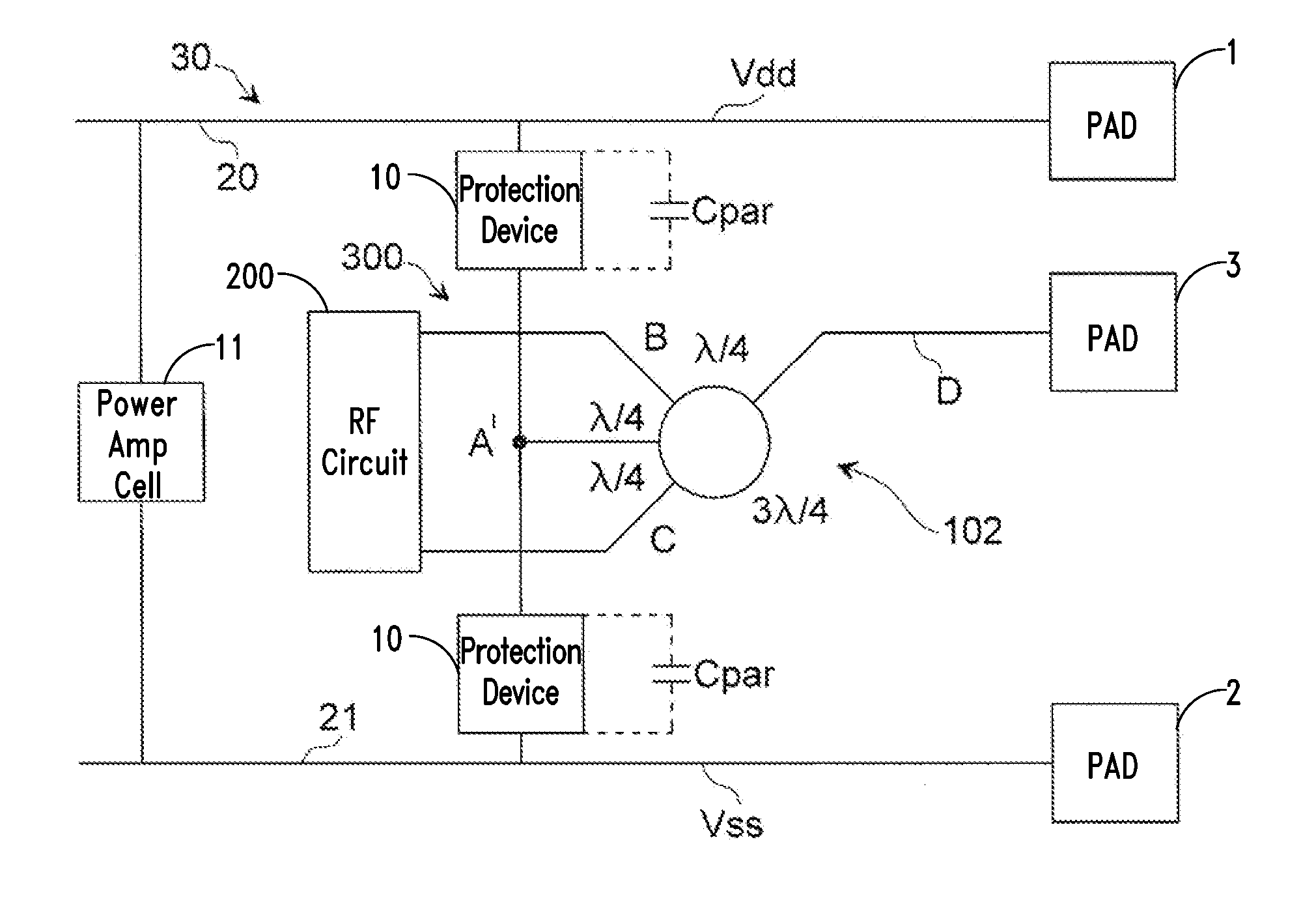
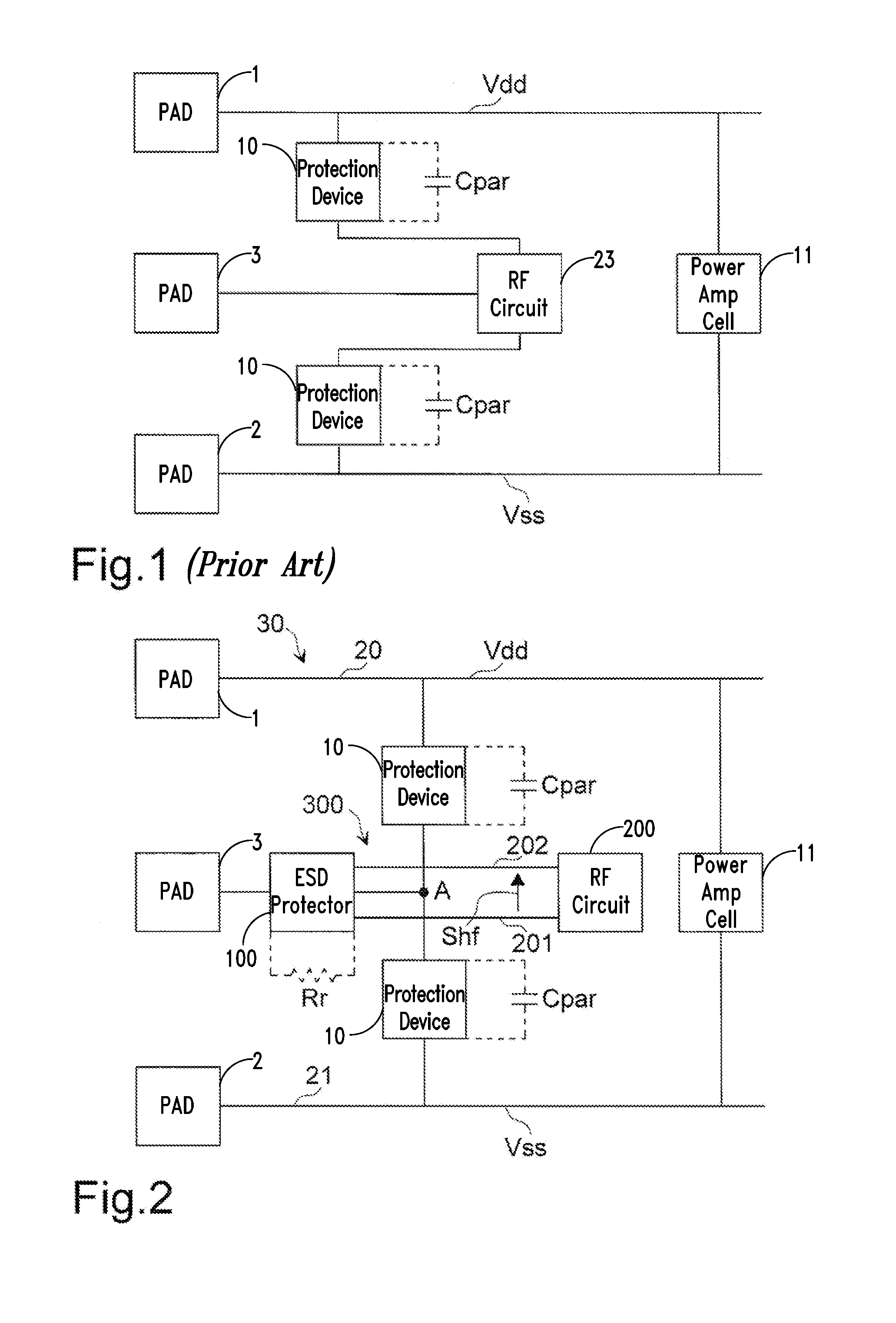
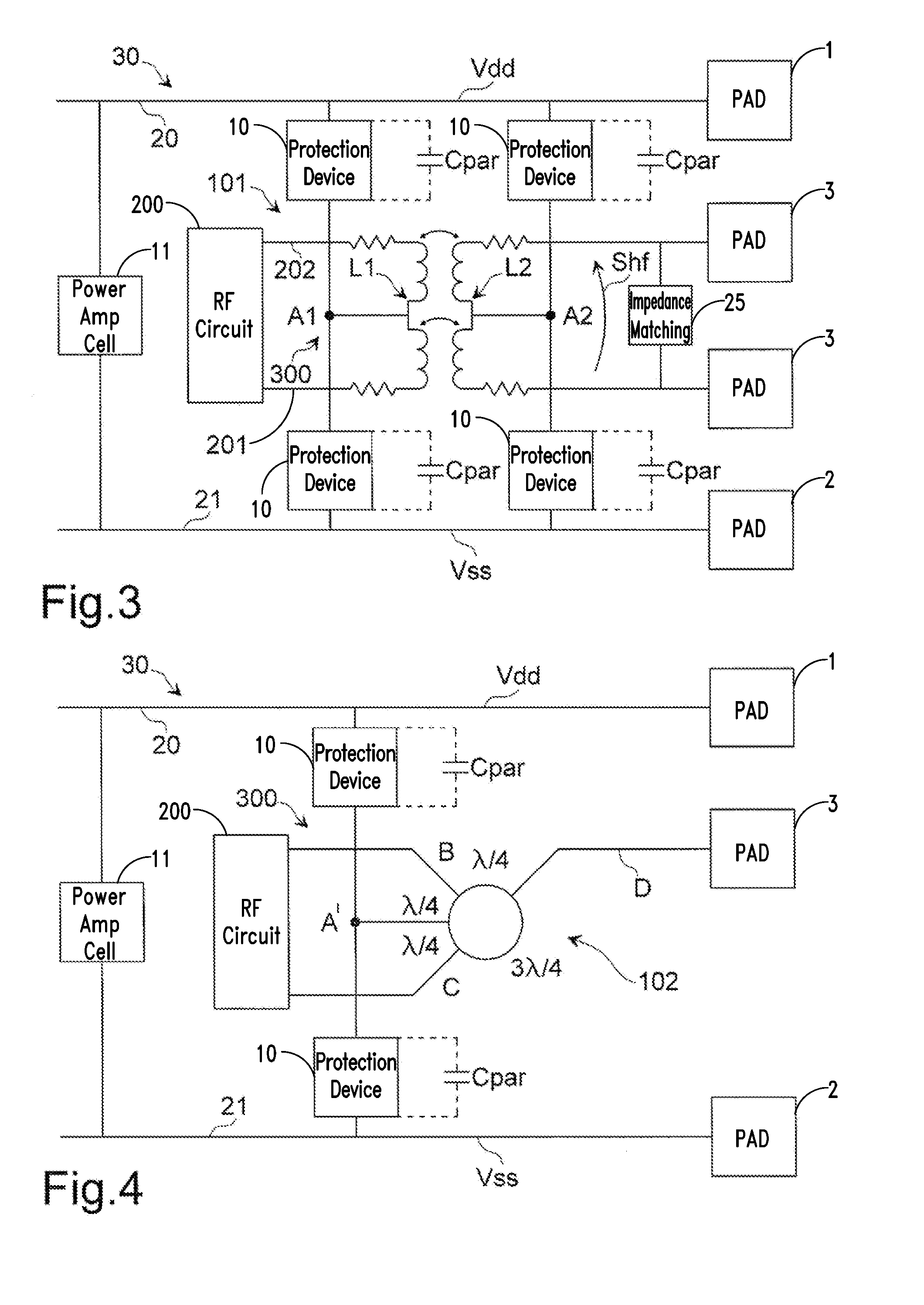
Referring to FIG. 2, there is shown a protection apparatus against electrostatic discharges for an integrated circuit in accordance with the present disclosure. The circuit of FIG. 2 comprises an integrated circuit 30, formed on a semiconductor substrate, for example silicon, and provided with PADs 1, 2 connected to the supply voltages Vdd and Vss with appropriate supply lines or paths 20, 21; the same two supply voltages Vdd and Vss are connected to each other by means of circuitry 11, referred to as “power clamp cell” that allows a discharge path for the PADs. The radiofrequency or higher frequency (for example microwave frequencies) internal circuit 200 is coupled to at least an output PAD 3 by an ESD protector 100. Protection devices 10 that protect against electrostatic discharges are connected to the supply voltages Vss and Vdd. Devices 10 and circuitry 11 belong to the protection apparatus that protects against electrostatic discharges for an integrated circuit in accordance ...


PUM


Abstract

There is described a protection apparatus against electrostatic discharges for an integrated circuit; said integrated circuit comprises a radiofrequency or higher frequencies internal circuit. The internal circuit has a first and a second terminals for the output or the input of a radiofrequency or higher frequencies signal. The apparatus comprises first means for electrically connecting said first and second terminals of the internal circuit to at least a PAD and the integrated circuit comprises at least a first and a second supply circuital lines and at least a first and a second protection devices against electrostatic discharges connected to said first and second supply lines. First means have a resistive component and each of said first and second protection devices against the electrostatic discharges have a parasitic capacitive component. The apparatus comprises second means configured to connect said first means and said first and second protection devices against the electrostatic discharges to at least a common circuital point preventing the resistive component of said first means or said internal circuit from combining with the parasitic capacitive components of said first and second protection devices against the electrostatic discharges.

Description

BACKGROUND1. Technical FieldThe present disclosure relates to a protection apparatus against electrostatic discharges for an integrated circuit and the related integrated circuit.2. Description of the Related ArtIntegrated circuits provide a high degree of functionality in a very small area, such functionalities may include a storage of data, processing of data, reception and transmission of radiofrequency data, etc. Integrated circuits typically comprise millions of transistors with sizes of the order of microns. It is known that bipolar and MOS transistors are subject to destructive breakdown phenomena when they undergo overvoltages due to electrostatic charges. For example, the gate oxide of a CMOS transistor, because of its minimal size, is susceptible to breakdown due to the static electricity, which is commonly referred to as electrostatic discharge or ESD. If one of the transistors of an integrated circuit is damaged by an electrostatic discharge or ESD, the integrated circui...

Claims


Application Information

Patent Timeline
IPC IPC(8): H02H9/00
CPCH01L23/645H01L23/66H01L27/0255H01L2924/3011H03F1/523H01L2924/0002H03F2200/441H01L2924/00
Inventor SCUDERI, ANGELOCALI, GIOVANNISCACCIANOCE, SALVATORE
Owner STMICROELECTRONICS SRL
Learn More