Eureka AIR delivers breakthrough ideas for toughest innovation challenges, trusted by R&D personnel around the world.

Devices and methods of protecting a cadmium sulfide for further processing

Inactive Publication Date: 2011-11-03
FIRST SOLAR INC (US)
View PDF0 Cites 7 Cited by
  • Summary
  • Abstract
  • Description
  • Claims
  • Application Information

AI Technical Summary

Benefits of technology

[0006]Methods are generally provided for protecting a cadmium sulfide layer on a substrate. In one particular embodiment, the method can include sputtering a cadmium sulfide layer onto a substrate from a cadmium sulfide target at a sputtering pressure (e.g., about 10 mTorr to about 150 mTorr), and sputtering a cap layer directly on the cadmium sulfide layer. The cap layer can be sputtered directly onto the cadmium sulfide layer without breaking vacuum of the sputtering pressure.

Problems solved by technology

However, the cadmium sulfide layer is susceptible to exposure to atmospheric contamination prior to deposition of subsequent layers (e.g., the cadmium telluride layer).
However, exposing the cadmium sulfide layer to air can adversely affect the interface between the cadmium sulfide layer and subsequent layers (e.g., a cadmium telluride layer) by introducing contaminants to the cadmium sulfide layer.

Method used


Image

  • Devices and methods of protecting a cadmium sulfide for further processing
  • Devices and methods of protecting a cadmium sulfide for further processing
  • Devices and methods of protecting a cadmium sulfide for further processing

Examples


Embodiment Construction

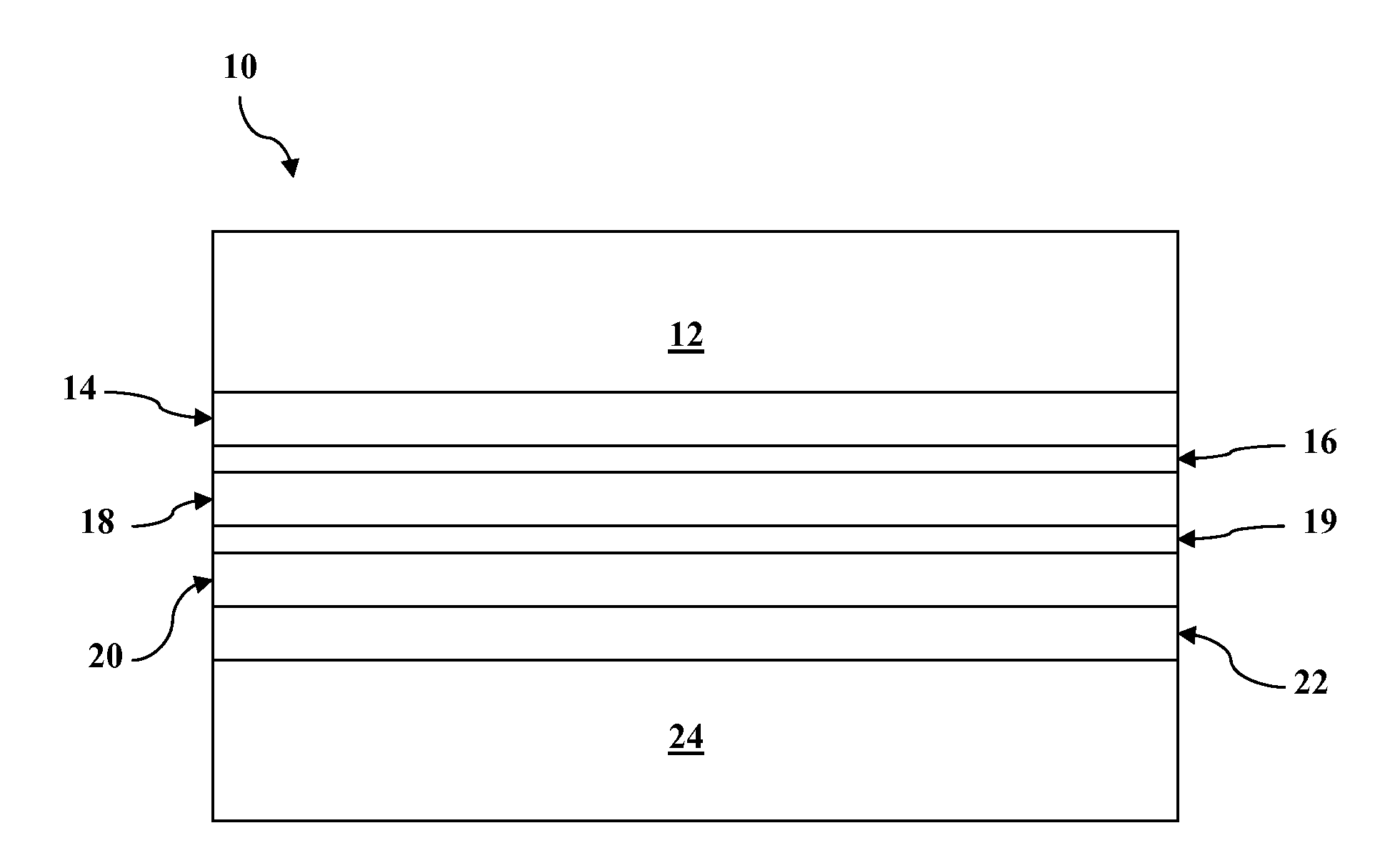
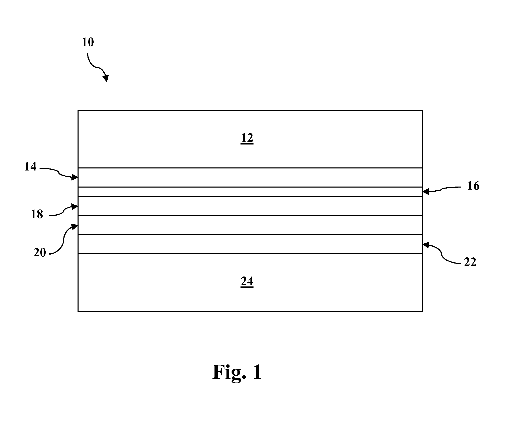
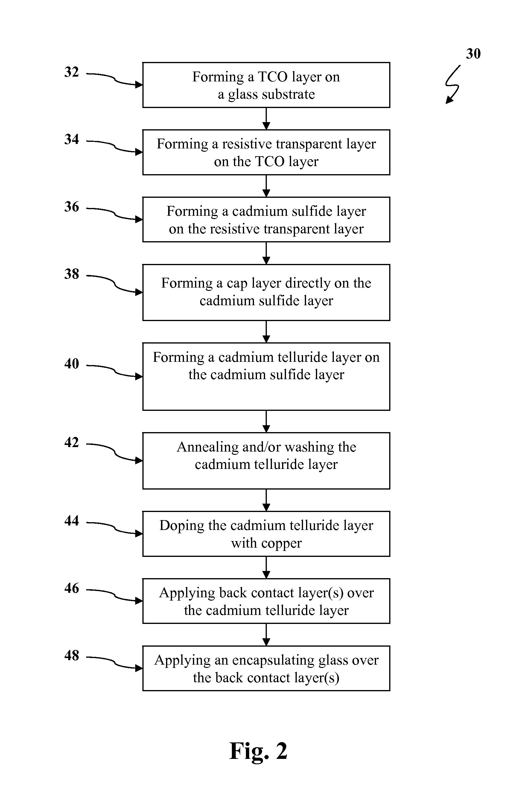
[0017]Reference now will be made in detail to embodiments of the invention, one or more examples of which are illustrated in the drawings. Each example is provided by way of explanation of the invention, not limitation of the invention. In fact, it will be apparent to those skilled in the art that various modifications and variations can be made in the present invention without departing from the scope or spirit of the invention. For instance, features illustrated or described as part of one embodiment can be used with another embodiment to yield a still further embodiment. Thus, it is intended that the present invention covers such modifications and variations as come within the scope of the appended claims and their equivalents.

[0018]In the present disclosure, when a layer is being described as “on” or “over” another layer or substrate, it is to be understood that the layers can either be directly contacting each other or have another layer or feature between the layers. Thus, the...


PUM

PropertyMeasurementUnit
Temperatureaaaaaaaaaa

Abstract

Methods for protecting a cadmium sulfide layer on a substrate are provided. The method can include sputtering a cadmium sulfide layer onto a substrate from a cadmium sulfide target at a sputtering pressure (e.g., about 10 mTorr to about 150 mTorr), and sputtering a cap layer directly on the cadmium sulfide layer. The cap layer can be sputtered directly onto the cadmium sulfide layer without breaking vacuum of the sputtering pressure. Methods are also provided for manufacturing a cadmium telluride based thin film photovoltaic device through depositing a cadmium sulfide layer on a substrate, depositing a cap layer directly on the cadmium sulfide layer, heating the substrate to sublimate at least a portion of the cap layer from the cadmium sulfide layer, and then depositing a cadmium telluride layer on the cadmium sulfide layer.An intermediate substrate for forming a cadmium telluride based thin-film photovoltaic device is also provided.

Description

FIELD OF THE INVENTION[0001]The subject matter disclosed herein relates generally to protecting a cadmium sulfide layer for further processing and protected cadmium sulfide layers. More particularly, the subject matter disclosed herein relates to methods of protecting a cadmium sulfide layer for use in the manufacture of cadmium telluride thin film photovoltaic devices.BACKGROUND OF THE INVENTION[0002]Thin film photovoltaic (PV) modules (also referred to as “solar panels”) based on cadmium telluride (CdTe) paired with cadmium sulfide (CdS) as the photo-reactive components are gaining wide acceptance and interest in the industry. CdTe is a semiconductor material having characteristics particularly suited for conversion of solar energy to electricity. For example, CdTe has an energy bandgap of about 1.45 eV, which enables it to convert more energy from the solar spectrum as compared to lower bandgap semiconductor materials historically used in solar cell applications (e.g., about 1.1 ...

Claims


Application Information

Patent Timeline
IPC IPC(8): H01L31/18H01L49/02
CPCC23C14/0629Y02E10/543H01L31/1836H01L31/073Y02P70/50
Inventor DRAYTON, JENNIFER ANNDEMARAY, RICHARD ERNEST
Owner FIRST SOLAR INC (US)
Why Eureka
Eureka Blog
Learn More