Multistage Demodulation Pixel and Method

a multi-stage demodulation and pixel technology, applied in the direction of exposure control, optical radiation measurement, instruments, etc., can solve problems such as inaccurate depth maps, and achieve the effect of reducing motion artifacts and improving performance in ambiguity-range or resolution

Active Publication Date: 2011-11-10
AMS SENSORS SINGAPORE PTE LTD
View PDF7 Cites 12 Cited by
  • Summary
  • Abstract
  • Description
  • Claims
  • Application Information

AI Technical Summary

Benefits of technology

[0013]The presented invention reduces these motion artifacts by appropriate pixel design and acquisition method.
[0014]Furthermore, the disclosed pixel architecture allows applying different modulation frequencies in the same exposure and storing samplings of these in the dedicated storage sites. This approach provides the possibility to use completely new demodulation schemes showing improved performance in ambiguity-range or in resolution for e.g. sine modulated system.

Problems solved by technology

However, another main challenge in the pixel design is to be able to sample at least three, preferably four times per period and store these samples in the pixel.
The process of deriving the depth information from the two acquired images results in an inaccurate depth map.

Method used


Image

  • Multistage Demodulation Pixel and Method
  • Multistage Demodulation Pixel and Method
  • Multistage Demodulation Pixel and Method

Examples


Embodiment Construction

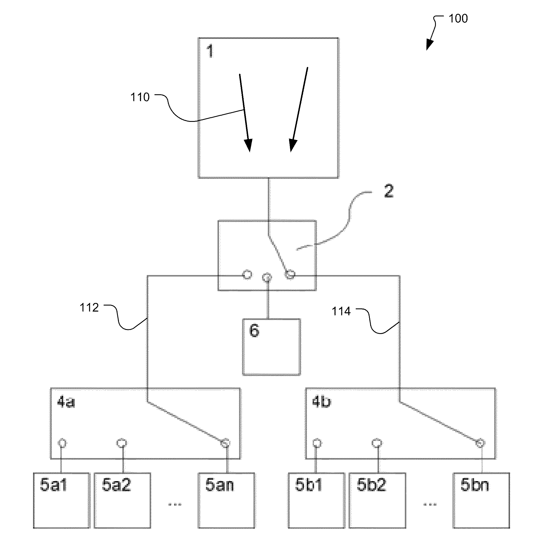
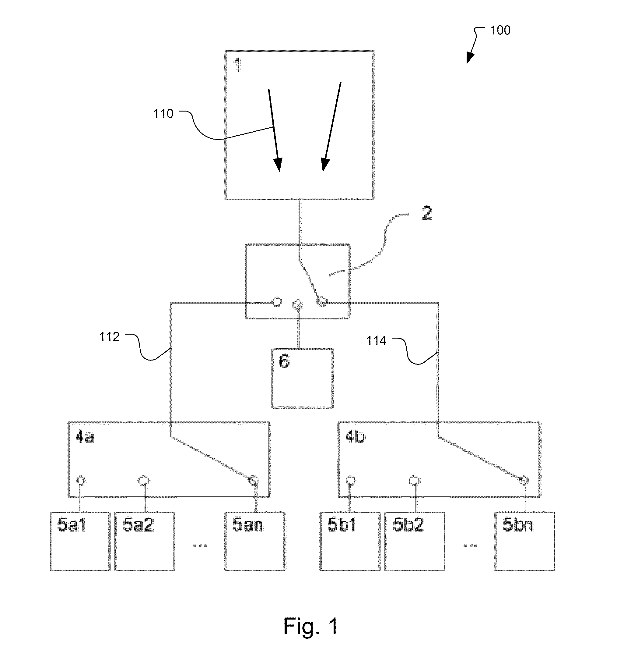
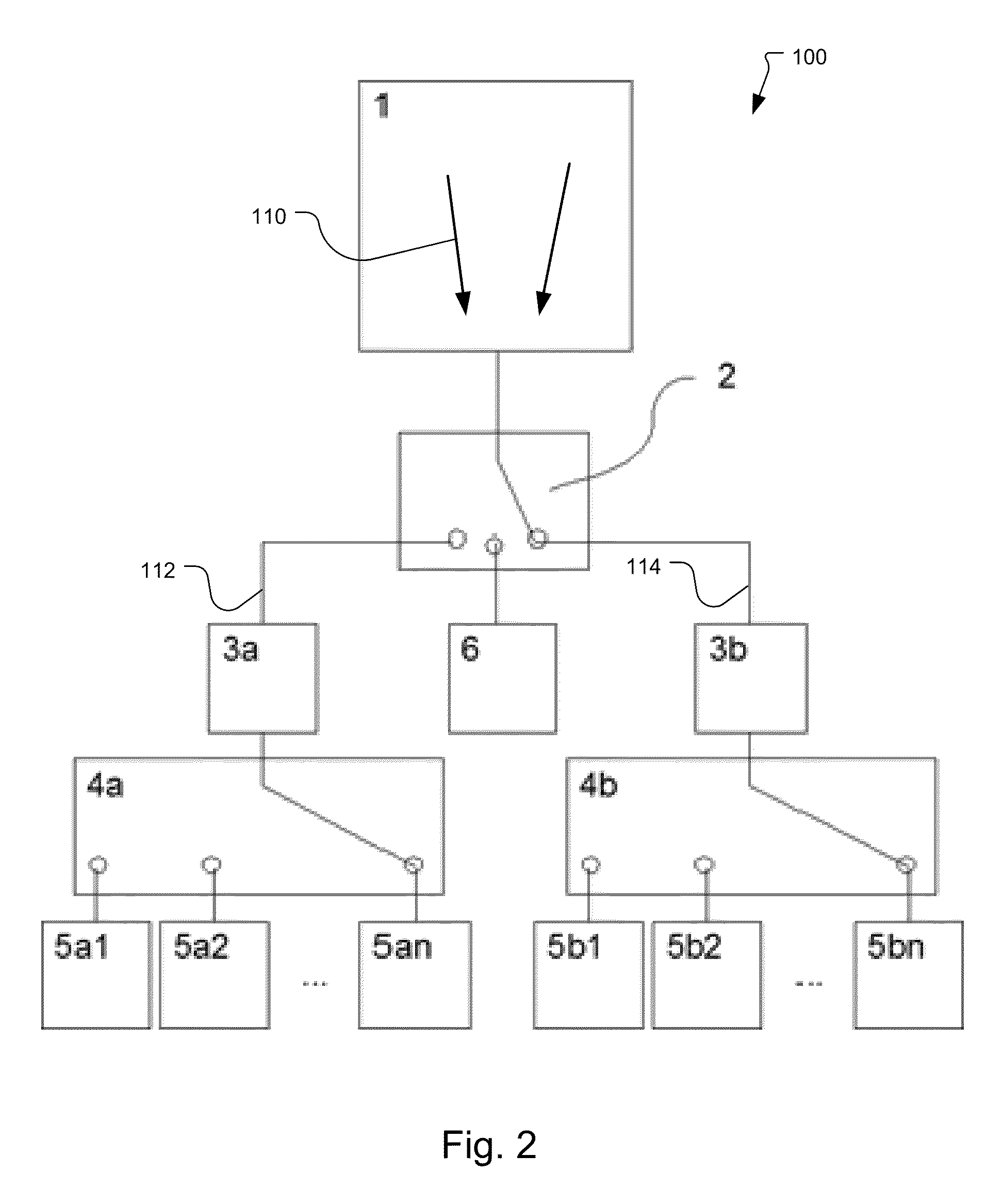
[0029]FIGS. 1 and 2 illustrate to demodulation pixels 100 that have been constructed according to the principles of the present invention.

[0030]The disclosed pixels 100 include at least one photo-sensitive area 1 that transfers the photo-charges quickly out of the photo-sensitive area. For this fast charge transport, a number of mechanisms are used in different implementations to generate a lateral drift field 110. In one implementation, the fast charge transport is provided by a series of gates or resistive gates as described in US 2008 / 0239466 A1, which is incorporated herein by this reference in its entirety. In another implementation, a pinned photo diode structure is used. In still other implementations, majority currents in the substrate or built-in drift fields are used. Still other mechanisms are possible. The key functionality is that photo-charges generated in the photosensitive area are transported in the direction of arrow 110 such as by a lateral drift field that is eit...


PUM


Abstract

A demodulation structure for a n-tap pixel, mainly for 3D time-of-flight (TOF) applications uses a 2-stage switch structure for demodulating a modulated electromagnetic wave. An almost arbitrary number of storage sites per pixel can be implemented enabling an almost arbitrary number of samplings captured during one exposure. It also provides the option to demodulate and integrate different phasing samples according to the different modulation frequencies within the same exposure.

Description

RELATED APPLICATIONS[0001]This application claims the benefit under 35 USC 119(e) of U.S. Provisional Application No. 61 / 259,333, filed on Nov. 9, 2009, which is incorporated herein by this reference in its entirety.BACKGROUND OF THE INVENTION[0002]The demodulation of modulated light signals at the pixel level requires in current approaches, the switching of a photo-generated charge current. Basically, both electron as well as hole currents are possible. The common methods use the photo-generated electron currents due to their higher mobility in the semiconductor material. Some pixel architectures do the necessary signal processing based on the photo-charge currents whereas other architectures work in the charge domain.[0003]Common to all pixels is the necessary transfer of photo-charges through the photo-sensitive detection region to a subsequent storage area or to a subsequent processing unit. In the case of charge-domain based pixel architectures, the photo-charge is generally tr...

Claims


Application Information

Patent Timeline
Patent Type & Authority Applications(United States)
IPC IPC(8): H04N7/18G01J1/42
CPCH04N5/37452G01S17/894H04N25/771
Inventor OGGIER, THIERRYLEHMANN, MICHAELBUETTGEN, BERNHARDFELBER, JONAS
Owner AMS SENSORS SINGAPORE PTE LTD
Why Eureka
Try Eureka