Semiconductor memory and method for manufacturing same

a technology of semiconductors and memory, applied in the field of semiconductor memory, can solve the problems of reducing unable to catch up with the rapid downscaling of lithography techniques, and difficulty in generation by generation to ensure the reliability and fast operation of nonvolatile memories. , to achieve the effect of increasing the bit density

Inactive Publication Date: 2011-11-24
KK TOSHIBA
View PDF5 Cites 703 Cited by
  • Summary
  • Abstract
  • Description
  • Claims
  • Application Information

AI Technical Summary

Benefits of technology

[0020]According to the invention, a semiconductor memory capable of increasing bit density by three-dimensional arrangement of cells, and a method for manufacturing the same can be realized.

Problems solved by technology

However, there are numerous problems to advance downscaling of flash memories also in the future.
(1) The development of lithography techniques cannot catch up with the rapid downscaling.
(2) Decreased device dimensions associated with downscaling cause the short channel effect and the narrow channel effect to sharply become pronounced, which has made it difficult generation by generation to ensure the reliability and fast operation of nonvolatile memories.
Because of the foregoing problems (1) to (3), it is probably difficult to continue increasing the bit density in the future by means of simple downscaling in a horizontal plane alone.
Hence, increase in the number of memory layers results in increasing the number of manufacturing steps, and also increasing manufacturing cost.
Thus, this technique has a problem with manufacturing cost per bit.

Method used


Image

  • Semiconductor memory and method for manufacturing same
  • Semiconductor memory and method for manufacturing same
  • Semiconductor memory and method for manufacturing same

Examples


first embodiment

[0119]At the outset, the invention is described.

[0120]This embodiment relates to a semiconductor memory, and more particularly to a nonvolatile semiconductor memory.

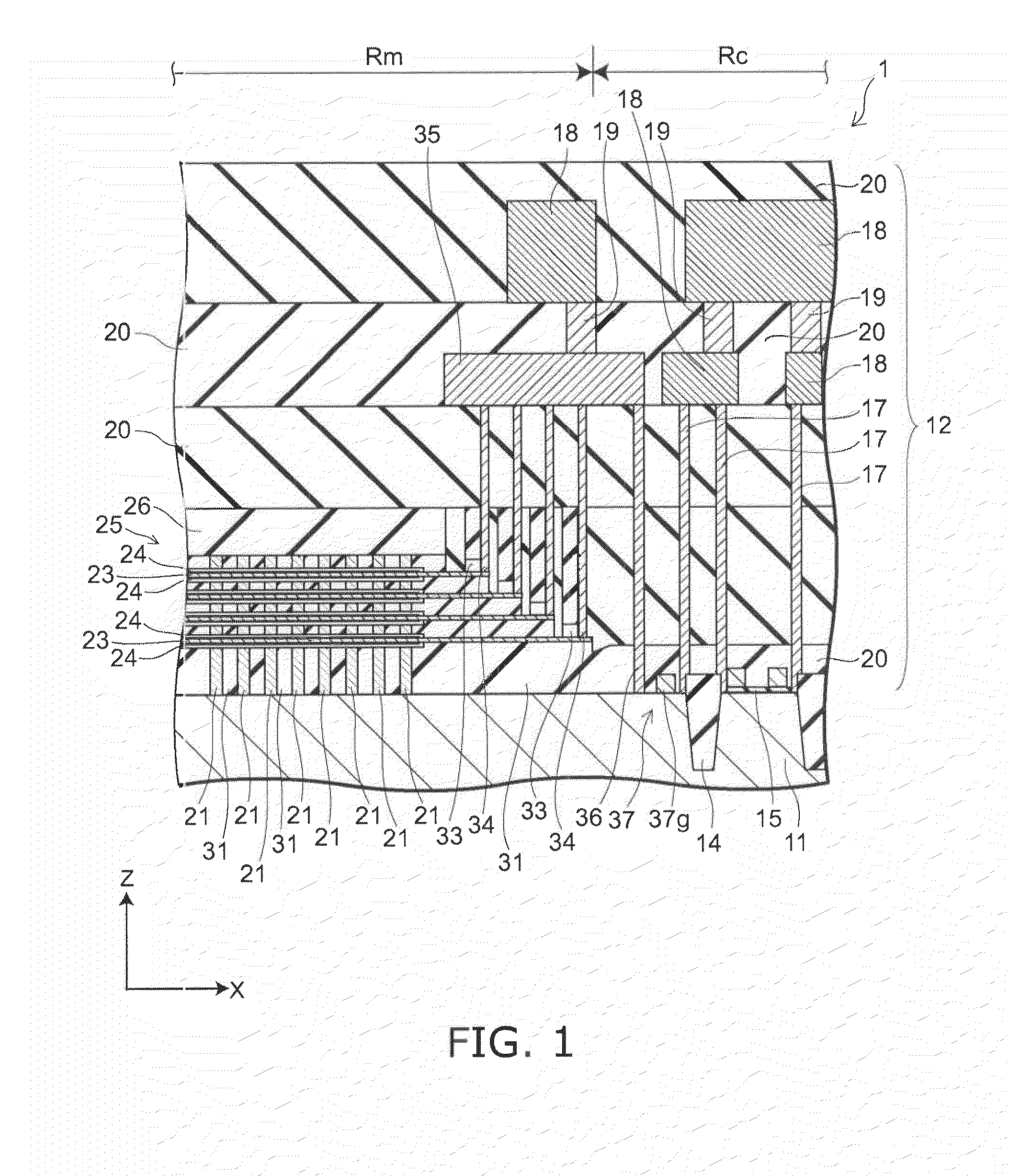
[0121]FIG. 1 is a cross-sectional view parallel to the extending direction of silicon beams illustrating the semiconductor memory according to this embodiment.

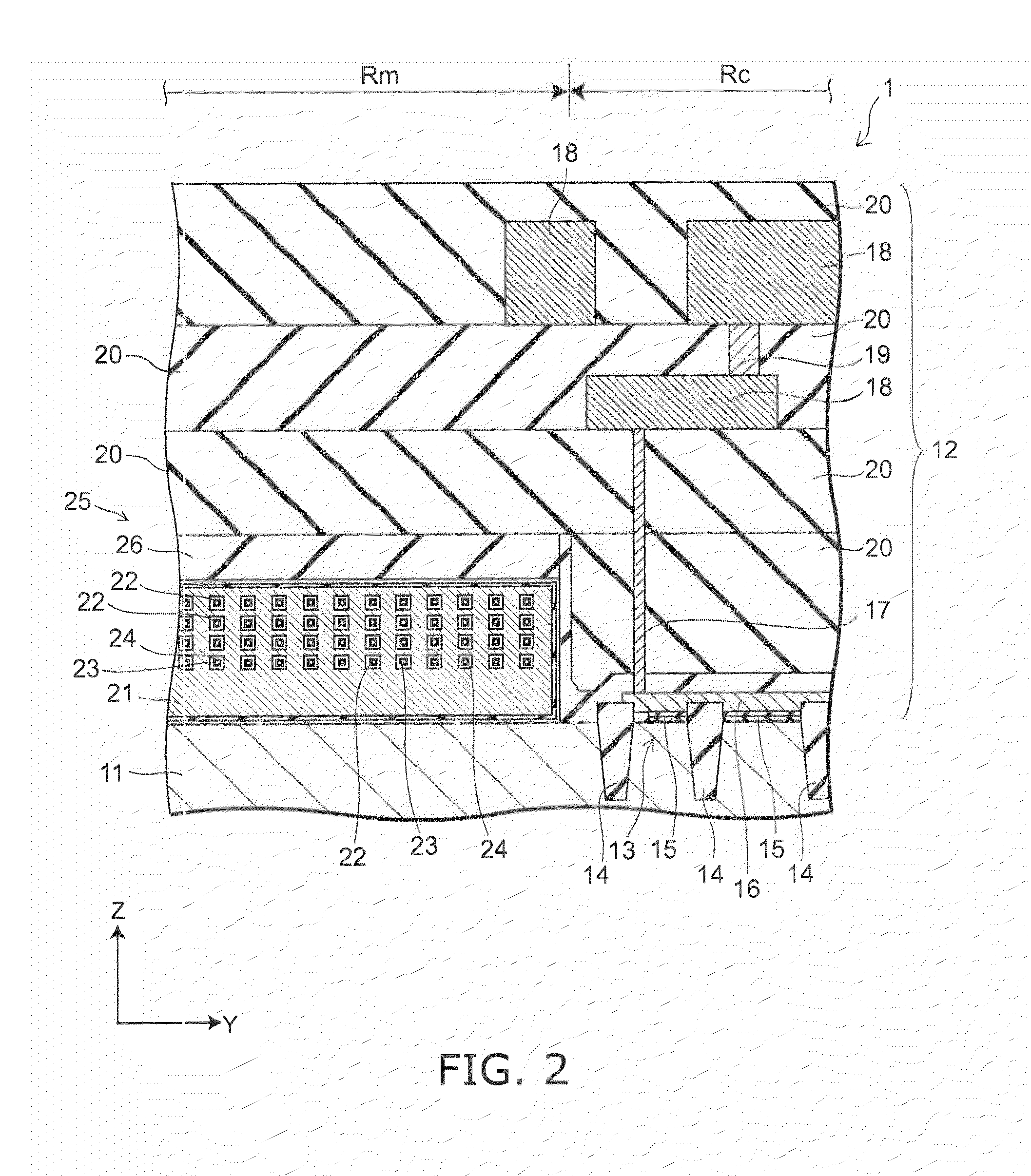
[0122]FIG. 2 is a cross-sectional view perpendicular to the extending direction of silicon beams illustrating the semiconductor memory according to this embodiment.

[0123]FIG. 3 is a cross-sectional perspective view illustrating the inside of the memory region of the semiconductor memory according to this embodiment.

[0124]FIG. 4 is a perspective view illustrating the gate electrode film and the silicon beam in the memory region of the semiconductor memory according to this embodiment.

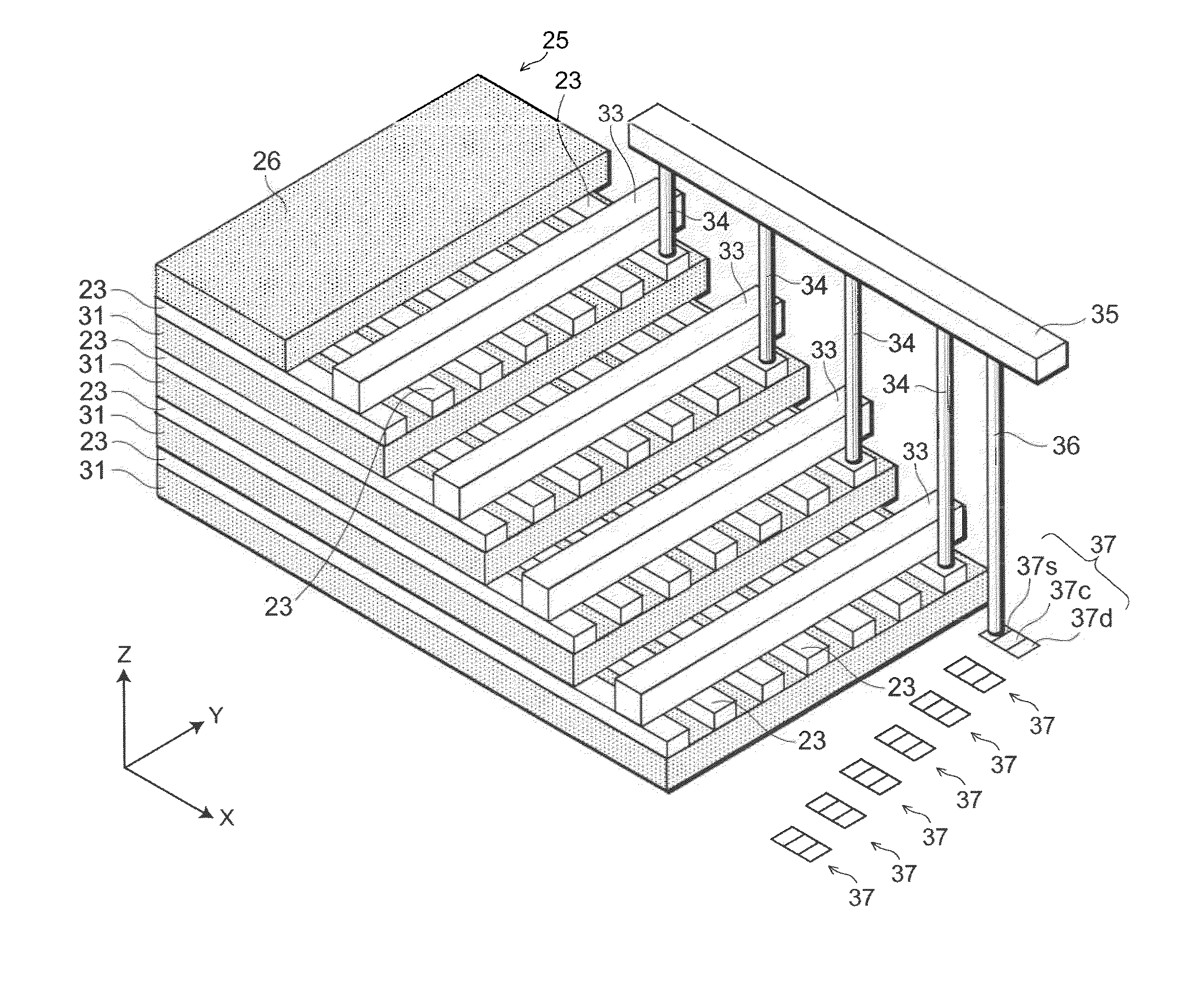
[0125]FIG. 5 is a cross-sectional view illustrating the basic unit of the structure body 25 in this embodiment.

[0126]FIG. 6 is a perspective view illustrating one end portion of the mem...

second embodiment

[0175]Next, the invention is described.

[0176]This embodiment relates to a first method for manufacturing the semiconductor memory according to the above first embodiment. This embodiment illustratively manufactures a 4-layer multilayer memory realizing a cell area of 900 nm2, which corresponds to the 1X nm generation in the conventional planar NAND flash memory. In this embodiment, the silicon beam constituting active areas (AA) is formed from polycrystalline silicon.

[0177]FIGS. 13A and 13B, 14A and 14B, 15A and 15B, 16A and 16B, and 17A and 17B are process cross-sectional views illustrating the method for manufacturing a semiconductor memory according to this embodiment, where FIGS. 13A, 14A, 15A, 16A, and 17A show the YZ cross section, and FIGS. 13B, 14B, 15B, 16B, and 17B show the XZ cross section.

[0178]FIGS. 18 to 21 are perspective cross-sectional views illustrating the method for manufacturing a semiconductor memory according to this embodiment.

[0179]First, as shown in FIGS. 1...

third embodiment

[0203]Next, the invention is described.

[0204]This embodiment relates to a second method for manufacturing the semiconductor memory according to the above first embodiment. This embodiment illustratively manufactures an 8-layer multilayer memory realizing a cell area of 450 nm2, which corresponds to the 0X nm generation in the conventional planar NAND flash memory. In this embodiment, the silicon beams constituting active areas (AA) are formed from epitaxial silicon.

[0205]FIG. 22 is a process cross-sectional view illustrating the method for manufacturing a semiconductor memory according to this embodiment.

[0206]FIGS. 23 to 27 are perspective cross-sectional views illustrating the method for manufacturing a semiconductor memory according to this embodiment.

[0207]In FIGS. 23 to 27, for simplicity of illustration, only six layers from the upper layer side of the multilayer body are shown.

[0208]First, as shown in FIG. 22, silicon germanium is epitaxially grown on a silicon substrate 201 ...


PUM


Abstract

A semiconductor memory capable of increasing bit density by three-dimensional arrangement of cells and a method for manufacturing the same are provided.In a semiconductor memory 1, gate electrode films 21 are provided on a silicon substrate 11. The gate electrode films 21 are arranged in one direction parallel to the upper surface of the silicon substrate 11 (X direction). Each gate electrode film 21 has a lattice plate-like shape, having through holes 22 in a matrix form as viewed in the X direction. Silicon beams 23 are provided passing through the through holes 22 of the gate electrode films 21 and extending in the X direction. Further, an ONO film 24 including a charge storage layer is provided between the gate electrode film 21 and the silicon beam 23.

Description

TECHNICAL FIELD[0001]This invention relates to a semiconductor memory and a method for manufacturing the same, and more particularly to a semiconductor memory including three-dimensionally arranged memory cells and a method for manufacturing the same.BACKGROUND ART[0002]Flash memories are widely used as high-capacity data storage in cellular phones, digital still cameras, USB (Universal Serial Bus) memories, silicon audio players and the like, and continuing to expand the market as the manufacturing cost per bit is reduced by rapid downscaling. Furthermore, novel applications have also been fast emerging, achieving a virtuous circle in which downscaling and manufacturing cost reduction find new markets.[0003]In particular, a NAND flash memory allows a plurality of active areas (hereinafter also referred to as “AA”) to share a gate conductor (hereinafter also referred to as “GC”), thereby substantially realizing cross-point cells having a cell area of 4F2, where F is the minimum proc...

Claims


Application Information

Patent Timeline
Patent Type & Authority Applications(United States)
IPC IPC(8): H01L29/792H01L21/20
CPCH01L27/11565H01L27/11582H01L27/11578H10B41/35H10B43/10H10B43/20H10B43/27H01L27/0688
Inventor KIYOTOSHI, MASAHIRO
Owner KK TOSHIBA
Why Eureka
Try Eureka