Semiconductor Package and Method for Making the Same

a technology of semiconductors and components, applied in the direction of electrical apparatus construction details, instruments, casings/cabinets/drawers, etc., can solve the problem of high yield rate, and achieve the effect of high yield rate and precise alignmen

Active Publication Date: 2011-11-24
ADVANCED SEMICON ENG INC
View PDF3 Cites 53 Cited by
  • Summary
  • Abstract
  • Description
  • Claims
  • Application Information

AI Technical Summary

Benefits of technology

[0011]The semiconductor package has the following advantages. First, there is no need of providing underfill in the semiconductor package, because there is no CTE mismatch issue. Second, there is no warpage concern for thin bridge chip. Third, the semiconductor package has precise alignment between the active chip and the bridge chip, and thus the yield rate is high.

Problems solved by technology

Third, the semiconductor package has precise alignment between the active chip and the bridge chip, and thus the yield rate is high.

Method used


Image

  • Semiconductor Package and Method for Making the Same
  • Semiconductor Package and Method for Making the Same
  • Semiconductor Package and Method for Making the Same

Examples


first embodiment

[0022]FIGS. 8 to 15 show a method for making a semiconductor package according to the present invention. Referring to FIGS. 8 and 9, a silicon substrate 20 is provided. The silicon substrate 20 comprises a plurality of silicon substrate units 21. Each silicon substrate unit 21 has a top surface 211, a bottom surface 212, a cavity 214 and a plurality of vias 213. The cavity 214 opens at the top surface 211, and the vias 213 penetrate the silicon substrate unit 21 and are disposed around the cavity 214. Preferably, each silicon substrate unit 21 further has at least one through hole 215 for venting air. One end of the through hole 215 opens at the bottom of the cavity 214, and the other end of the through hole 215 opens at the bottom surface 212 of the silicon substrate unit 21. Referring to FIG. 10, a plurality of glue layers 22 are formed in the cavities 214.

[0023]Referring to FIG. 11, a plurality of bridge chips 23 are provided. Each bridge chip 23 has an active surface 231, a back...

second embodiment

[0036]FIGS. 16 to 23 show another method for making a semiconductor package according to the present invention. Referring to FIGS. 16 and 17, a silicon substrate 30 is provided. The silicon substrate 30 comprises a plurality of silicon substrate units 31. Each silicon substrate unit 31 has a top surface 311, a bottom surface 312, a cavity 314 and a plurality of vias 313. The cavity 314 opens at the top surface 311, and the vias 313 penetrate the silicon substrate unit 31 and are disposed around the cavity 314. Preferably, each silicon substrate unit 31 further has at least one through hole 315 for venting air. One end of the through hole 315 opens at the bottom of the cavity 314, and the other end of the through hole 315 opens at the bottom surface 312 of the silicon substrate unit 31. Referring to FIG. 18, a plurality of glue layers 32 are formed in the cavities 314.

[0037]Referring to FIG. 19, a plurality of bridge chips 33 are provided. Each bridge chip 33 has an active surface 33...

third embodiment

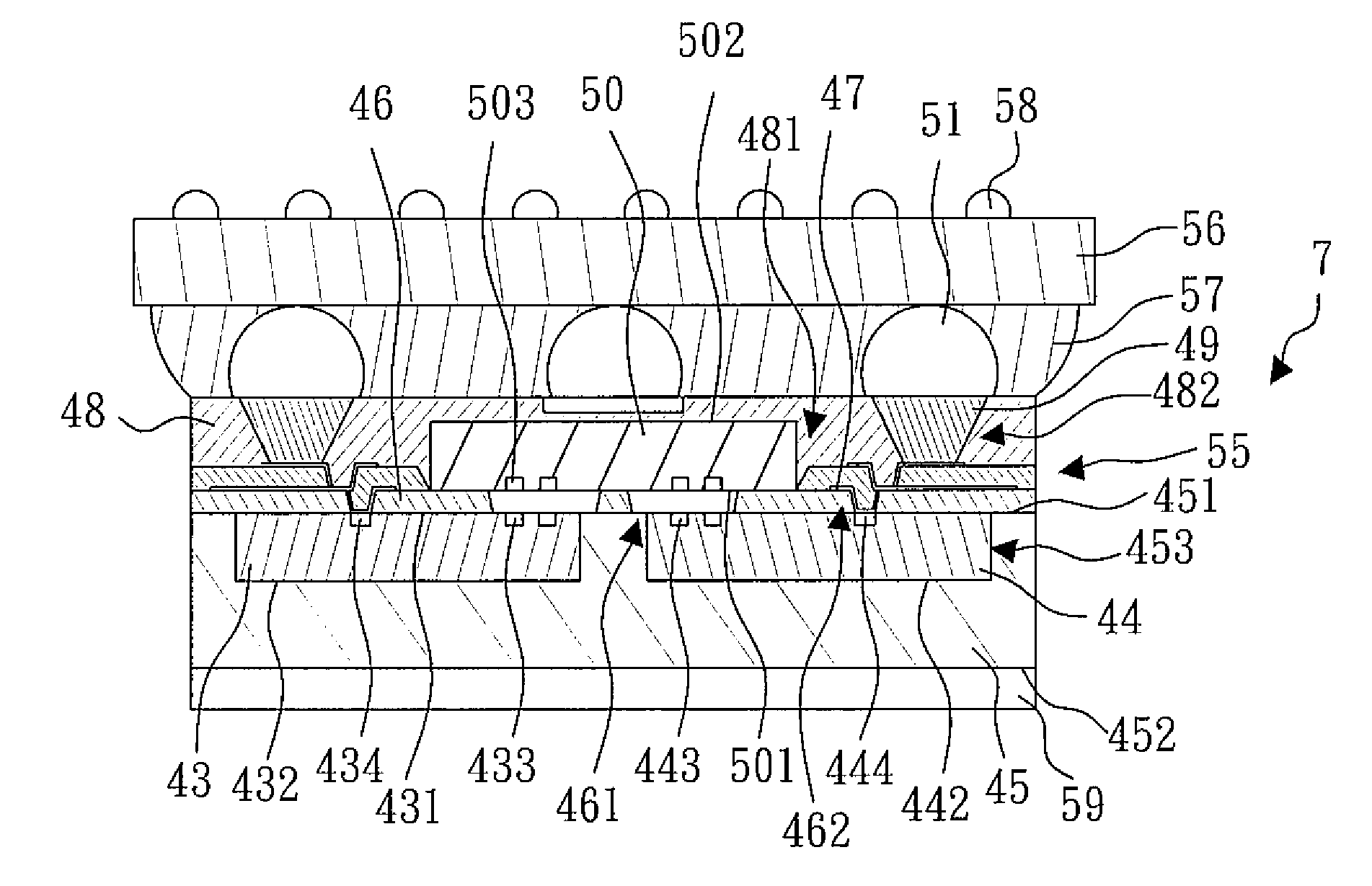
[0047]FIGS. 24 to 37 show a method for making a semiconductor package according to the present invention. Referring to FIG. 24, a carrier 41 is provided. In the embodiment, the carrier 41 is a wafer having a release film 42 thereon. Referring to FIG. 25, a plurality of active chips 43, 44 are provided. The active chip 43 has a has an active surface 431, a back surface 432, a plurality of non-contact pads 433 and a plurality of conducting pads 434. The non-contact pads 433 and conducting pads 434 are disposed adjacent to the active surface 431. The active chip 44 has a has an active surface 441, a back surface 442, a plurality of non-contact pads 443 and a plurality of conducting pads 444. The non-contact pads 443 and conducting pads 444 are disposed adjacent to the active surface 441. Then, the active surfaces 431, 441 of the active chips 43, 44 are attached to the carrier 41. In the embodiment, the active surfaces 431, 441 of the active chips 43, 44 are attached to the release film...


PUM


Abstract

The present invention relates to a semiconductor package and method for making the same. The semiconductor package includes a silicon substrate unit, a bridge chip and at least one active chip. The silicon substrate unit has a cavity and a plurality of vias. The bridge chip is attached to the cavity and has a plurality of non-contact pads. The active chip is disposed above the bridge chip and has a plurality of non-contact pads and a plurality of conducting elements. The conducting elements of the active chip contact the vias of the silicon substrate unit, the non-contact pads of the active chip face but are not in physical contact with the non-contact pads of the bridge chip, so as to provide proximity communication between the active chip and the bridge chip.

Description

BACKGROUND OF THE INVENTION[0001]1. Field of the Invention[0002]The present invention relates to a semiconductor package and method for making the same, and more particularly to a semiconductor package having the function of proximity communication and method for making the same.[0003]2. Description of the Related Art[0004]FIGS. 1 to 7 show a conventional method for making a semiconductor package. Referring to FIG. 1, a first active chip 10 and a bridge chip 11 are provided. The first active chip 10 has an active surface 101, a back surface 102, a plurality of bumps 103 and a plurality of non-contact pads 104. The non-contact pads 104 and the bumps 103 are disposed adjacent to the active surface 101. The bridge chip 11 has an active surface 111, a back surface 112 and a plurality of non-contact pads 113. The non-contact pads 113 are disposed adjacent to the active surface 111.[0005]Referring to FIG. 2, the first active chip 10 and the bridge chip 11 are bonded together by a glue lay...

Claims


Application Information

Patent Timeline
Patent Type & Authority Applications(United States)
IPC IPC(8): H01L23/538H01L21/78H01L21/50
CPCH01L23/13H01L2924/014H01L23/48H01L23/49816H01L23/49827H01L23/5389H01L24/24H01L24/82H01L25/0652H01L2224/24227H01L2225/06517H01L2225/06531H01L2924/01029H01L2924/15153H01L2924/15165H01L23/3128H01L2924/01019H01L2924/01006H01L2924/01005H01L24/96H01L2224/04105H01L2224/12105H01L2224/96
Inventor WENG, CHAO-FUWU, YI-TING
Owner ADVANCED SEMICON ENG INC
Why Eureka
Try Eureka