Light emitting diode package

a technology of light-emitting diodes and packages, applied in the direction of basic electric elements, electrical equipment, semiconductor devices, etc., can solve the problems of ceramic materials that can experience cracking during sintering

Inactive Publication Date: 2011-12-01
ADVANCED OPTOELECTRONICS TECH
View PDF6 Cites 33 Cited by
  • Summary
  • Abstract
  • Description
  • Claims
  • Application Information

AI Technical Summary

Problems solved by technology

Many plastic leaded chip carriers (PLCCs) cannot tolerate the high temperature

Method used


Image

  • Light emitting diode package
  • Light emitting diode package
  • Light emitting diode package

Examples


first embodiment

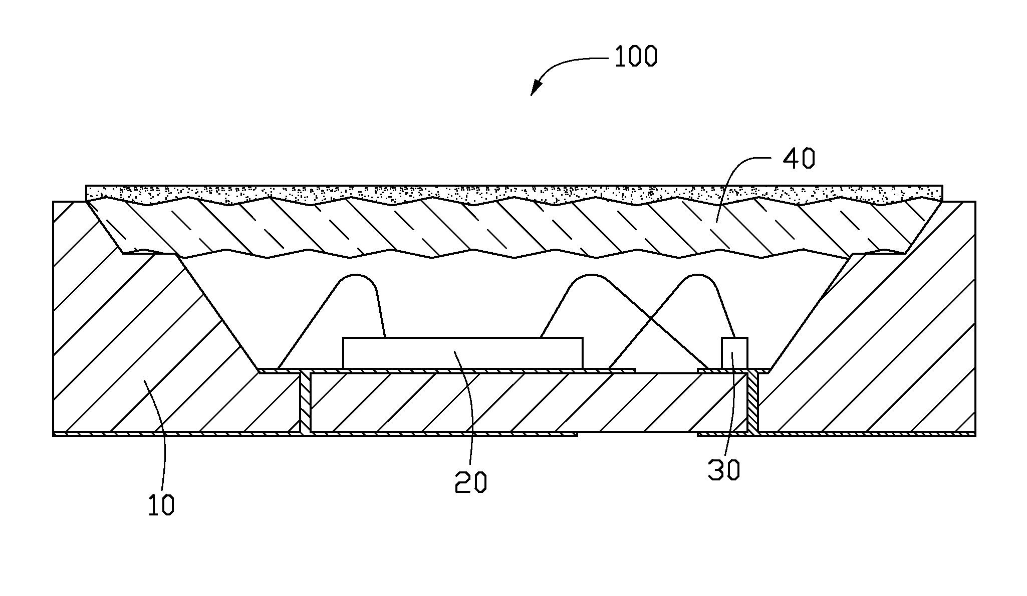
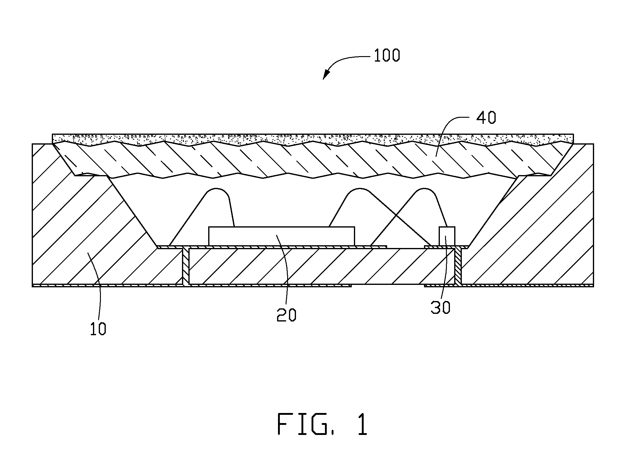
[0014]Referring to FIG. 1, it shows a light emitting diode package 100 in accordance with the disclosure. The light emitting diode package 100 includes a substrate 10, a light emitting diode chip 20, a voltage stabilization diode 30 such as a zener diode, and a lens 40, wherein the light emitting diode chip 20 and the voltage stabilization diode 30 are fixed on the substrate 10, and the lens 40 covers the light emitting diode chip 20 and the voltage stabilization diode 30.

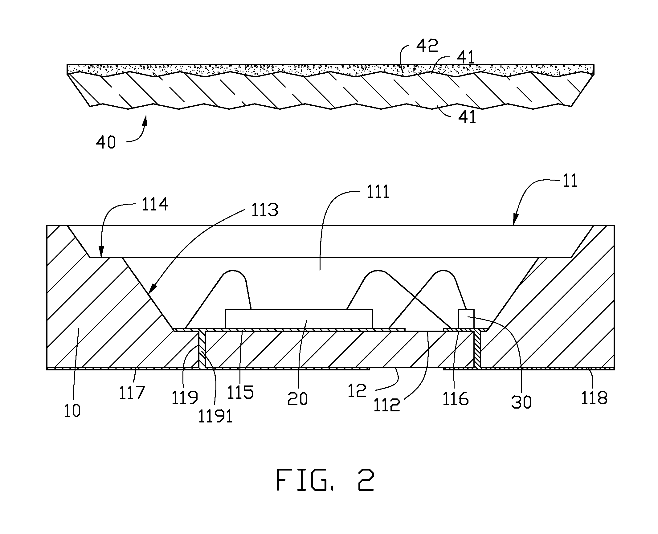
[0015]FIG. 2 is a view similar to FIG. 1, with the lens 40 separating from the substrate 10 of the light emitting diode package 100. The substrate 10 is a silicon substrate which has high or low electrical resistance. The silicon substrate 10 with high electrical resistance has an electrical resistivity of about 1 to 30000 Ω / cm and can be doped with boron or phosphor. The silicon substrate 10 with low electrical resistance has an electrical resistivity of about 0.001 to 0.02 Ω / cm and can be doped with boron, phosph...

third embodiment

[0021]FIG. 4 is a cross section of a light emitting diode package 100b in accordance with the disclosure. The light emitting diode package 100b has a cavity 111 which is filled by a fluorescent material 50, wherein the fluorescent material 50 is made of a mixture consisting of transparent gel and fluorescent powers. The transparent gel can be silicone, epoxy, or other transparent materials. The fluorescent material 50 not only can convert light from the light emitting diode chip 20 and absorbed thereby to another light having a different wavelength, but also can seal the light emitting diode chip 20 to prevent moisture from environment.

fourth embodiment

[0022]Referring to FIG. 5, it shows a cross section of a light emitting diode package 100c in accordance with the disclosure. The light emitting diode package 100c includes a lens 40c which has an arc-shaped configuration, wherein the lens 40c has concave 43 formed facing to the light emitting diode chip 20. The lens 40c is disposed on the platform 114 of the cavity 111 of the silicon substrate 10. The fluorescent conversion layer 42 can be disposed on a convex, top surface of the lens 40c.


PUM


Abstract

A light emitting diode package includes a silicon substrate having a first surface and a second surface opposite to the first surface, wherein the first surface includes a cavity, a light emitting diode chip fixed on a bottom of the cavity, and a glass lens secured to the silicon substrate and covering the light emitting diode chip.

Description

BACKGROUND[0001]1. Technical Field[0002]The disclosure relates generally to light emitting diodes, and more particularly to a light emitting diode package with high thermal tolerance.[0003]2. Description of the Related Art[0004]Accompanying increased intensity and luminosity, LED chips generate increased heat to consume than before, especially to high power LED chips. Many plastic leaded chip carriers (PLCCs) cannot tolerate the high temperature, and ceramic materials can experience cracking during sintering and packaging. Therefore, it is desired to provide an LED package which can overcome the described limitations.BRIEF DESCRIPTION OF THE DRAWINGS[0005]FIG. 1 is a cross section of a light emitting diode package in accordance with a first embodiment of the disclosure.[0006]FIG. 2 is a view similar to FIG. 1, with a lens being separated from the light emitting diode package.[0007]FIG. 3 is a cross section of the lens of the light emitting diode package in accordance with a second e...

Claims


Application Information

Patent Timeline
IPC IPC(8): H01L33/58
CPCH01L33/486H01L33/641H01L2924/01322H01L2224/45144H01L2224/45124H01L2224/48227H01L2224/48091H01L2924/00014H01L2924/00H01L2224/45139H01L2224/48237H01L2924/00011H01L2924/181H01L2924/01004H01L2924/00012H01L2224/45015H01L2924/207
Inventor HSIEH, MIN-TSUNTSENG, WEN-LIANGCHEN, LUNG-HSINLIN, CHIH-YUNG
Owner ADVANCED OPTOELECTRONICS TECH
Why Eureka
Try Eureka