

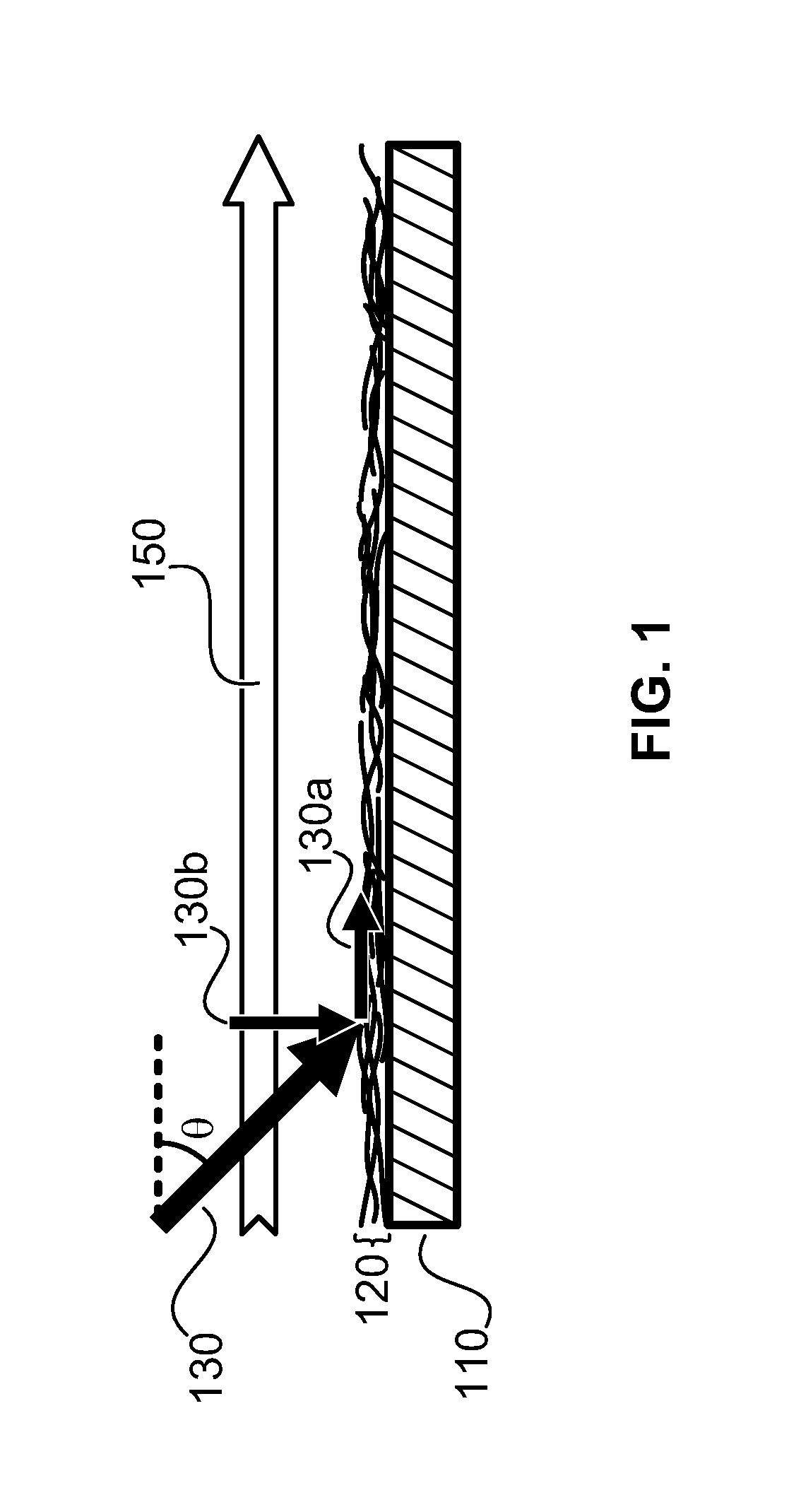
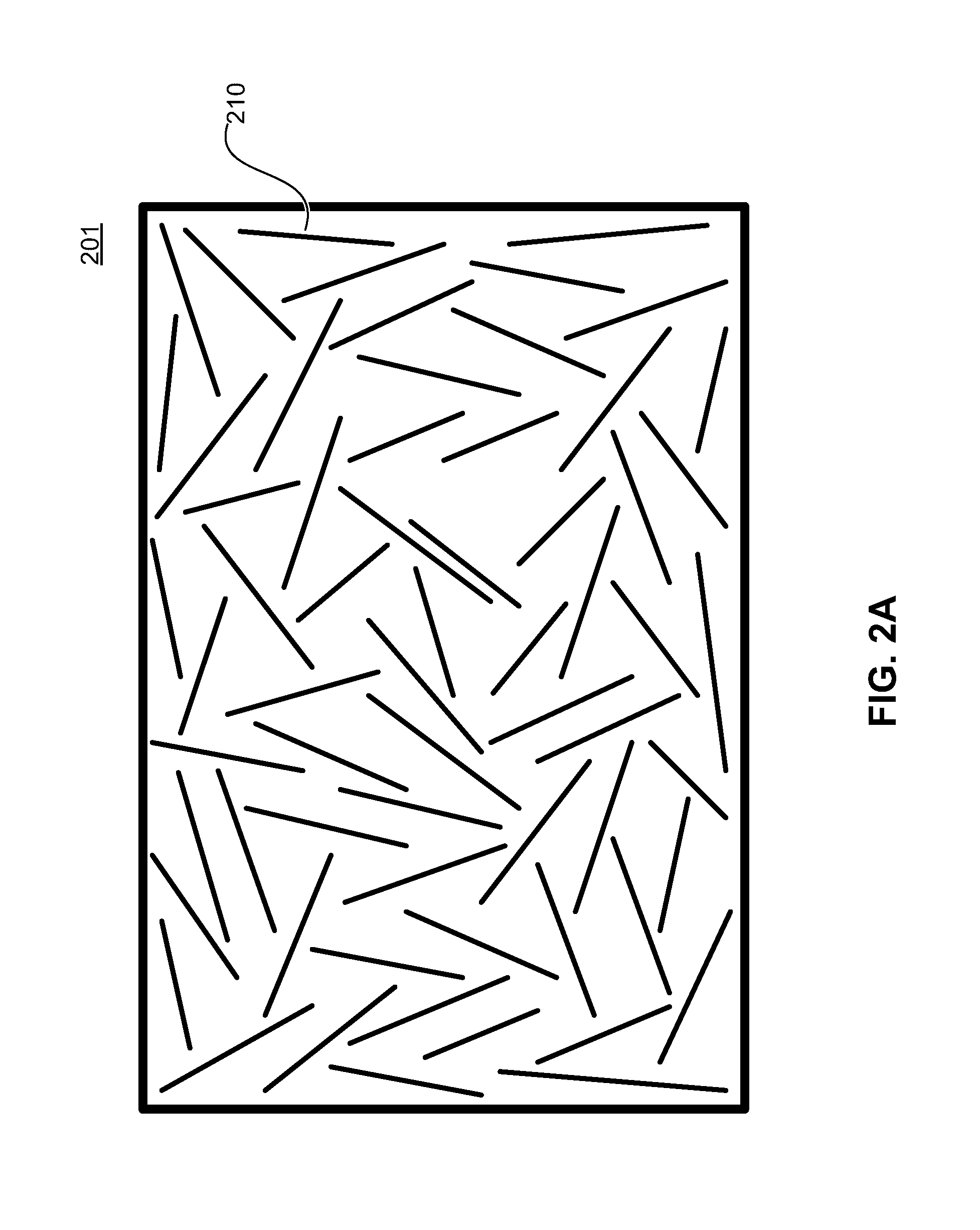
Methods for arranging nanoscopic elements within networks, fabrics, and films
a technology of nanotubes and layers, applied in the field of nanotube fabric layers and films, can solve the problems of small scale nanotube arrangement techniques, commercial applications, and inability to adapt to any large scale, and achieve the effect of not being practical for the arrangement of nanotube elements in large scale films and fabrics
- Summary
- Abstract
- Description
- Claims
- Application Information
AI Technical Summary
Benefits of technology
Problems solved by technology
Method used
Image

Examples
example 1
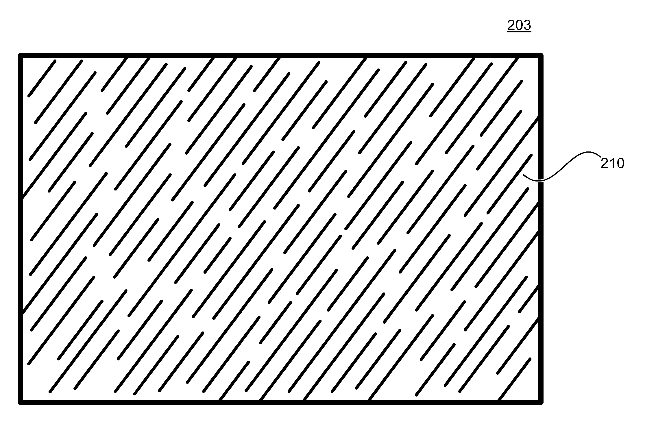
[0201]FIGS. 19A-19C are SEM images of an exemplary nanotube fabric layer at different magnifications (1901, 1902, and 1903 respectively) first formed via three spin coating operations of a purified nanotube application solution (as described above) and then rendered into an ordered network of nanotube elements through the application of a directional rolling force along the direction indicated within each SEM image. The rolling force was applied via a steel hand roller, rolled directly against the nanotube fabric layer fifty times with light pressure (approximately two Newtons). As is evident in FIG. 19A (the 10,000× magnification image), the resulting nanotube fabric layer was rendered into an ordered state oriented along the direction of the applied rolling force.
example 2
[0202]FIGS. 20A-20C are SEM images of an exemplary nanotube fabric layer at different magnifications (2001, 2002, and 2003 respectively) first formed via three spin coating operations of a purified nanotube application solution (as described above) and then rendered into an ordered network of nanotube elements through the application of a directional rubbing force along the direction indicated within each SEM image. The rubbing force was applied by placing the wafer facedown on a TEFLON or polytetrafluoroethylene sheet (such that the nanotube fabric layer was in direct contact with the TEFLON or polytetrafluoroethylene sheet), placing a 150 g weight on the reverse side (that is, the non-coated side) of the wafer, and sliding the wafer along the TEFLON or polytetrafluoroethylene sheet a distance of approximately five inches fifteen times. As is evident in FIG. 20A (the 5,000× magnification image), the nanotube fabric layer exhibited thin bands (on the order of 2 μm across) of ordered...
example 3
[0203]FIGS. 21A-21C are SEM images of an exemplary nanotube fabric layer at different magnifications (2101, 2102, and 2103 respectively) first formed via three spin coating operations of a purified nanotube application solution (as described above) and then rendered into an ordered network of nanotube elements through the application of a directional rubbing force along the direction indicated within each SEM image. The rubbing force was applied by placing the wafer facedown on a TEFLON or polytetrafluoroethylene sheet (such that the nanotube fabric layer was in direct contact with the TEFLON or polytetrafluoroethylene sheet), placing a 150 g weight on the reverse side (that is, the non-coated side) of the wafer, and sliding the wafer along the TEFLON or polytetrafluoroethylene sheet a distance of approximately five inches twenty-five times. As is evident in FIG. 21A (the 5,000× magnification image), the resulting nanotube fabric layer was rendered into an ordered state oriented alo...
PUM
| Property | Measurement | Unit |
|---|---|---|
| stroke length | aaaaa | aaaaa |
| stroke length | aaaaa | aaaaa |
| stroke length | aaaaa | aaaaa |
Abstract
Description
Claims
Application Information