High power density betavoltaic battery

a betavoltaic battery and high-power technology, applied in the field of semiconductor devices, devices and semiconductor device packaging, plus batteries, can solve the problems of poor efficiency, insufficient open circuit voltage or power conversion efficiency of betavoltaic devices made from si, and poor efficiency. achieve the effect of high-power density betavoltaic batteries

Active Publication Date: 2011-12-08
WIDETRONIX
View PDF11 Cites 29 Cited by
  • Summary
  • Abstract
  • Description
  • Claims
  • Application Information

AI Technical Summary

Problems solved by technology

Thus, betavoltaic devices made from Si are suboptimal, due to this poor efficiency.
Silicon (Si), the semiconductor industry workhorse, cannot realize sufficiently high open circuit voltages or power conversion efficiencies to be an optimal alternative for beta-voltaic batteries.
Although the Curie load is calculated from the total volume of the radioactive material, the amount of useable energy is limited to the number of high energy electrons which escape from the surface of the source before they can be reabsorbed.

Method used


Image

  • High power density betavoltaic battery
  • High power density betavoltaic battery
  • High power density betavoltaic battery

Examples


Embodiment Construction

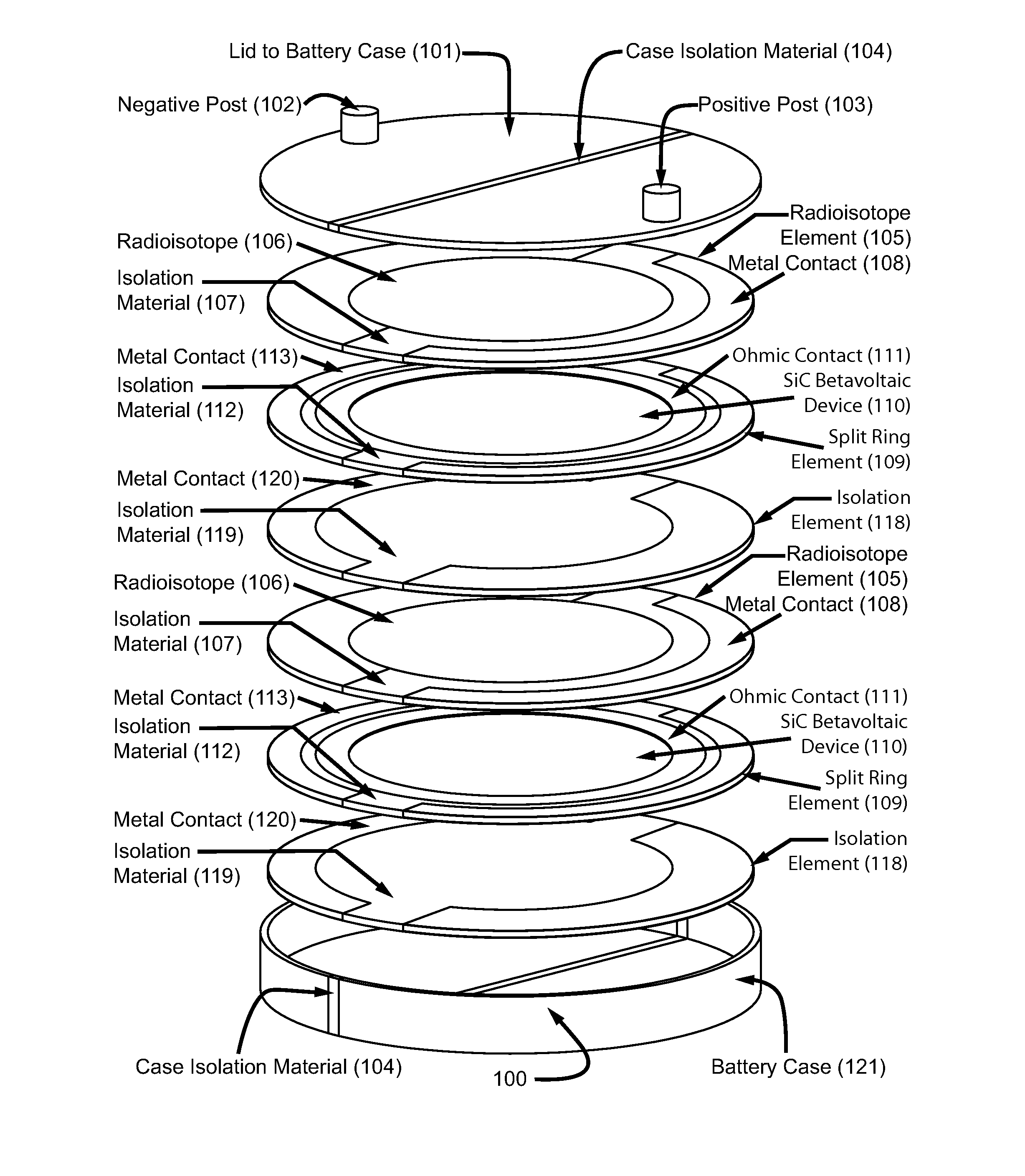
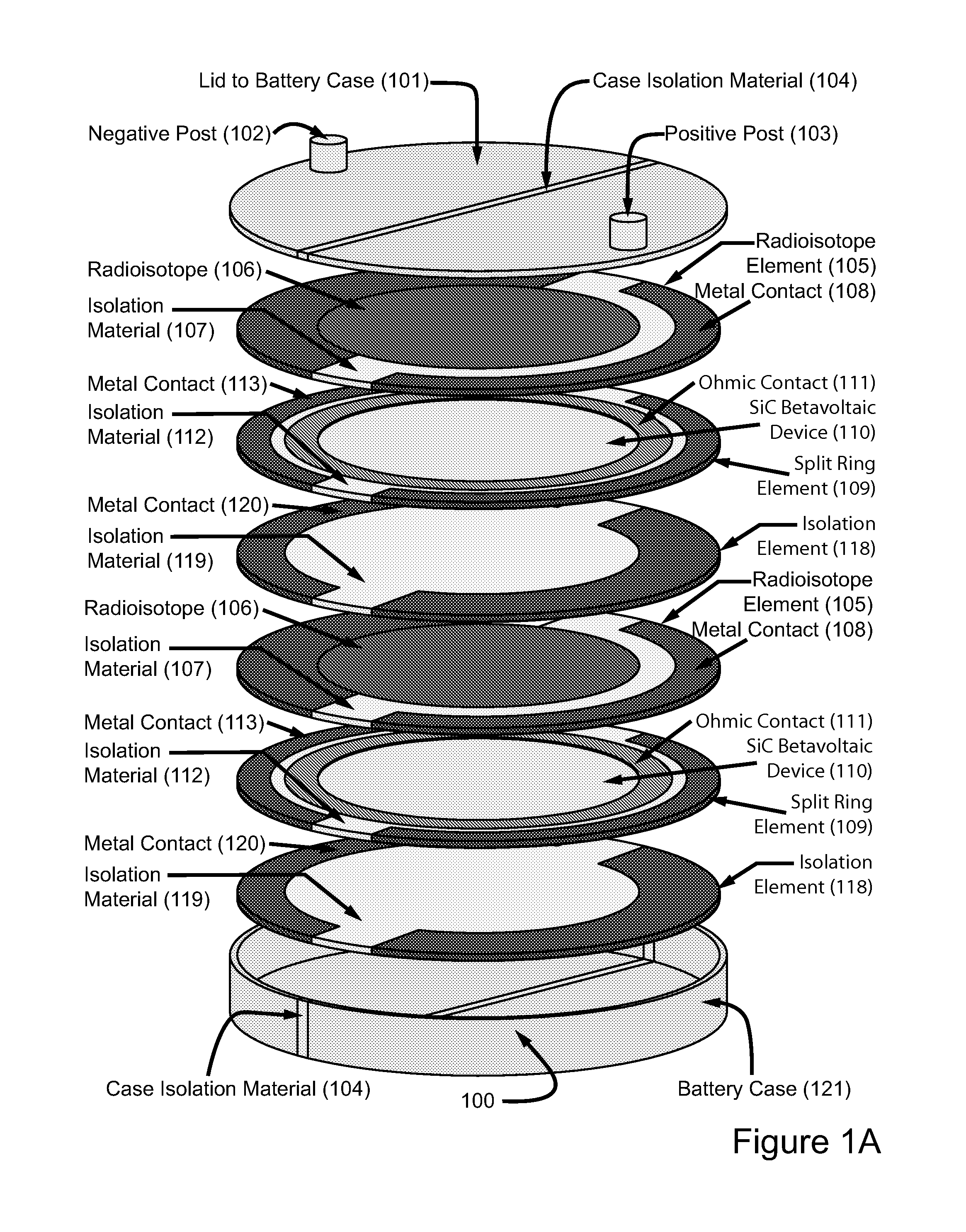
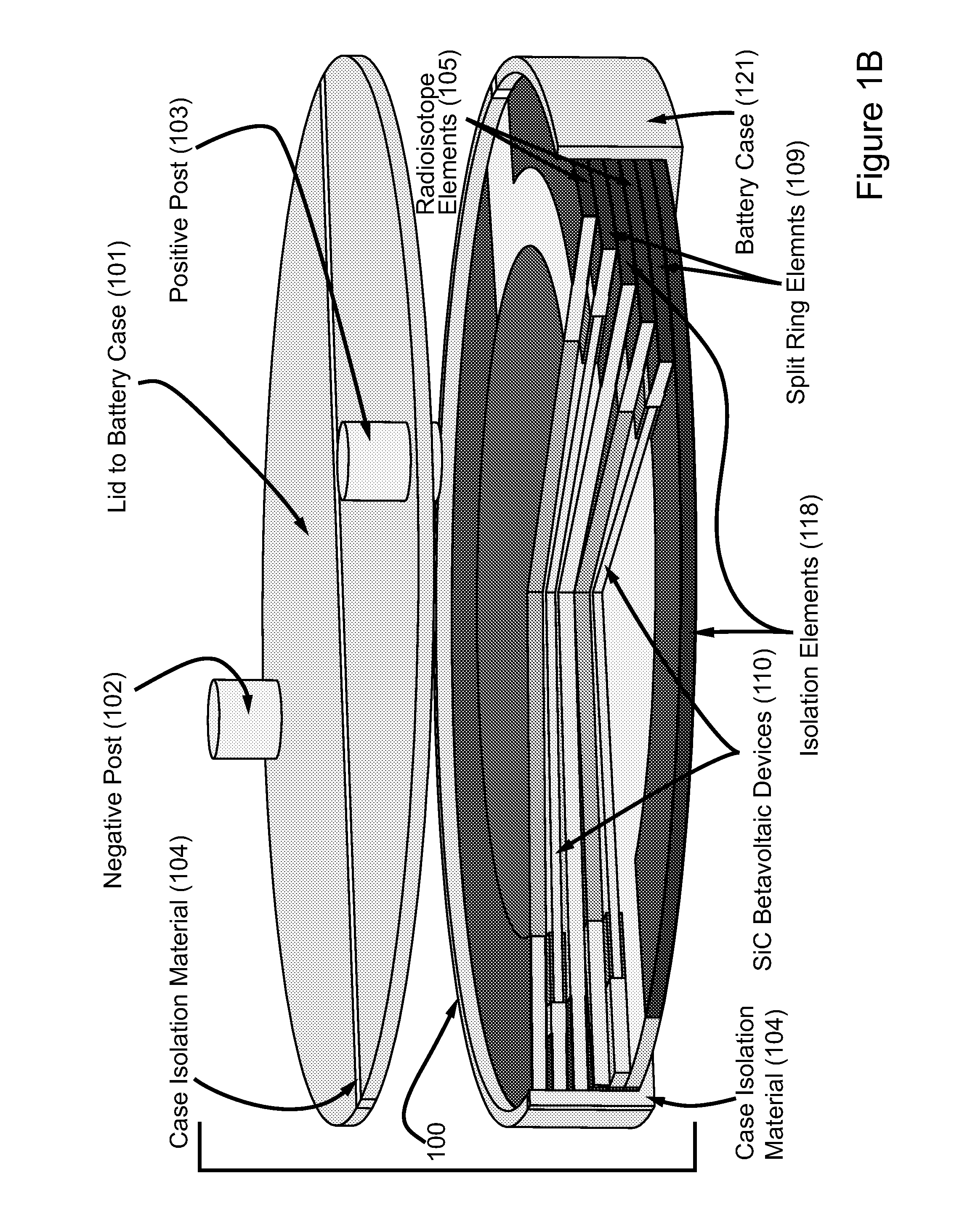
[0023]One embodiment of the invention is a circularly symmetric implementation, as shown in FIGS. 1 and 3. Square geometry, as shown in FIG. 2, may be employed, as well. Other geometries may be used to fit the application of interest.

[0024]The device is assembled one layer at a time, using various elements described below. This assembly may be performed manually or with robotic aid.

[0025]In one embodiment, the device is assembled in a case whose core is comprised of insulating material, such as aluminum oxide, and is plated with magnetic shielding material. Shielding materials, such as Fe, Ni, u (Mu)-Metal or any other material with a high magnetic susceptibility, may be used to screen stray and intentionally applied magnetic fields. The inside of the case is insulated to prevent device shorting.

[0026]In a further embodiment, the device is assembled in a case whose core is also comprised of insulating material such as aluminum oxide and is plated with electrical shielding material. ...


PUM


Abstract

To increase total power in a betavoltaic device, it is desirable to have greater radioisotope material and / or semiconductor surface area, rather than greater radioisotope material volume. An example of this invention is a high power density betavoltaic battery. In one example of this invention, tritium is used as a fuel source. In other examples, radioisotopes, such as Nickel-63, Phosphorus-33 or promethium, may be used. The semiconductor used in this invention may include, but is not limited to, Si, GaAs, GaP, GaN, diamond, and SiC. For example (for purposes of illustration / example, only), tritium will be referenced as an exemplary fuel source, and SiC will be referenced as an exemplary semiconductor material. Other variations and examples are also discussed and given.

Description

[0001]This is a Continuation of (based on) a U.S. Provisional Application Ser. No. 61 / 231,863, filed on 6 Aug. 2009, with the same title, assignee, and inventors.FIELD OF THE INVENTION[0002]The field of the invention relates to semiconductor materials, devices and semiconductor device packaging, plus batteries.BACKGROUND OF THE INVENTION[0003]Beta-voltaic devices have very high energy density and utilize radioisotopes as a fuel source. Radioisotope emissions originate from within a few microns of a radioactive material's surface at very low levels (nW / cm2-μW / cm2), despite the high power density in the bulk of the radioactive source (mW / cc-W / cc). Several semiconductor materials, such as Si, GaAs, GaP, GaN and diamond, may be used in betavoltaic devices.[0004]However, silicon carbide (SiC) is the material used here for the production of beta voltaic devices, due to its wide bandgap. Moreover, in addition to its radiation hardness and ability not to degrade over time at higher temperat...

Claims


Application Information

Patent Timeline
Patent Type & Authority Applications(United States)
IPC IPC(8): H01L29/66
CPCH01L31/115G21H1/06
Inventor SPENCER, MICHAELCHANDRASHEKHAR, MVS
Owner WIDETRONIX
Why Eureka
Try Eureka