
Methodology for forming pnictide compositions suitable for use in microelectronic devices

a technology of microelectronic devices and compositions, which is applied in the direction of crystal growth process, polycrystalline material growth, coatings, etc., can solve the problems of poor photovoltaic behavior of devices, poor film quality, and difficulty in preparing n-type zinc phosphide, and achieves excellent control of growth rate and composition, enhances the safety of using deposition strategies, and is used more easily and effectively

Inactive Publication Date: 2015-05-19
DOW GLOBAL TECH LLC +1
View PDF10 Cites 0 Cited by
  • Summary
  • Abstract
  • Description
  • Claims
  • Application Information

AI Technical Summary

Benefits of technology

[0009]The present invention offers many advantages. The method allows excellent control over growth rate and composition of the resulting thin films. Composition characteristics can be controlled on demand to grow uniform, single layer films. Alternatively, films can be made from multiple sublayers with differing compositions, optionally with p-type or n-type characteristics as desired. Single or multilayer stacks may be grown using one or more ingredient(s) including at least one single source compound in a single chamber as composition can be controlled in many embodiments by appropriate processing of the vapor flux rather than of the source compound. Thus, in some modes of practice, one can create all or a portion of a junction from the same source compound in a single process chamber using strategies described herein.
[0010]Composition characteristics can also be controlled via process control strategies in order to help ensure that films are grown in a manner that meets composition objectives. Deriving pnictogen content from one or more compound sources greatly enhances the safety of using deposition strategies to grow pnictogen-containing films for microelectronic applications. The techniques allow more efficient use of pnictogen so that more pnictogen ends up in the desired film rather than as by-product. The methods also allow higher temperatures to be used more easily and effectively for metal and pnictogen delivery to the growing film.

Problems solved by technology

Preparing n-type zinc phosphide, particularly using methodologies suitable for the industrial scale, remains challenging.
However, such approaches generally yield devices with poor photovoltaic behavior, if any, due at least in part to poor film quality, lack of control over film stoichiometry, and / or lack of control over formation of high quality p / n junctions.

Method used


Image

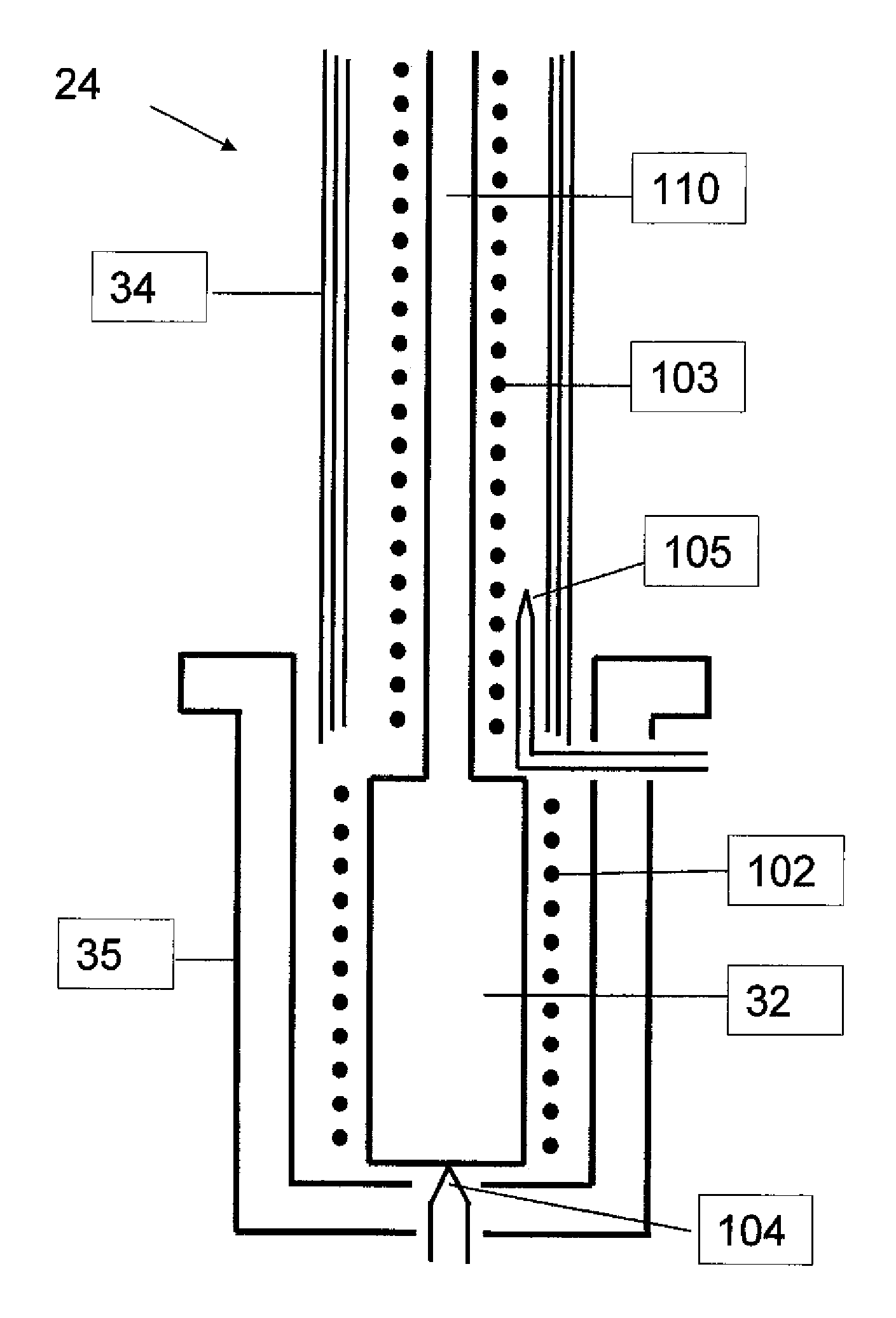
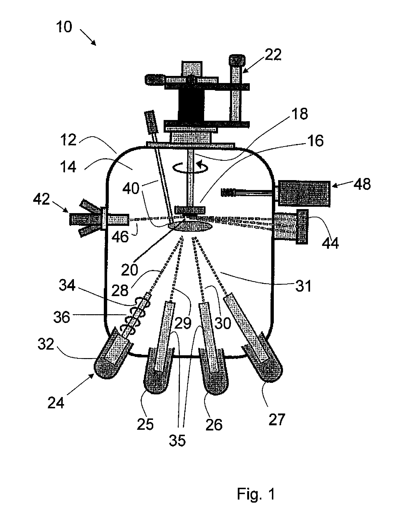
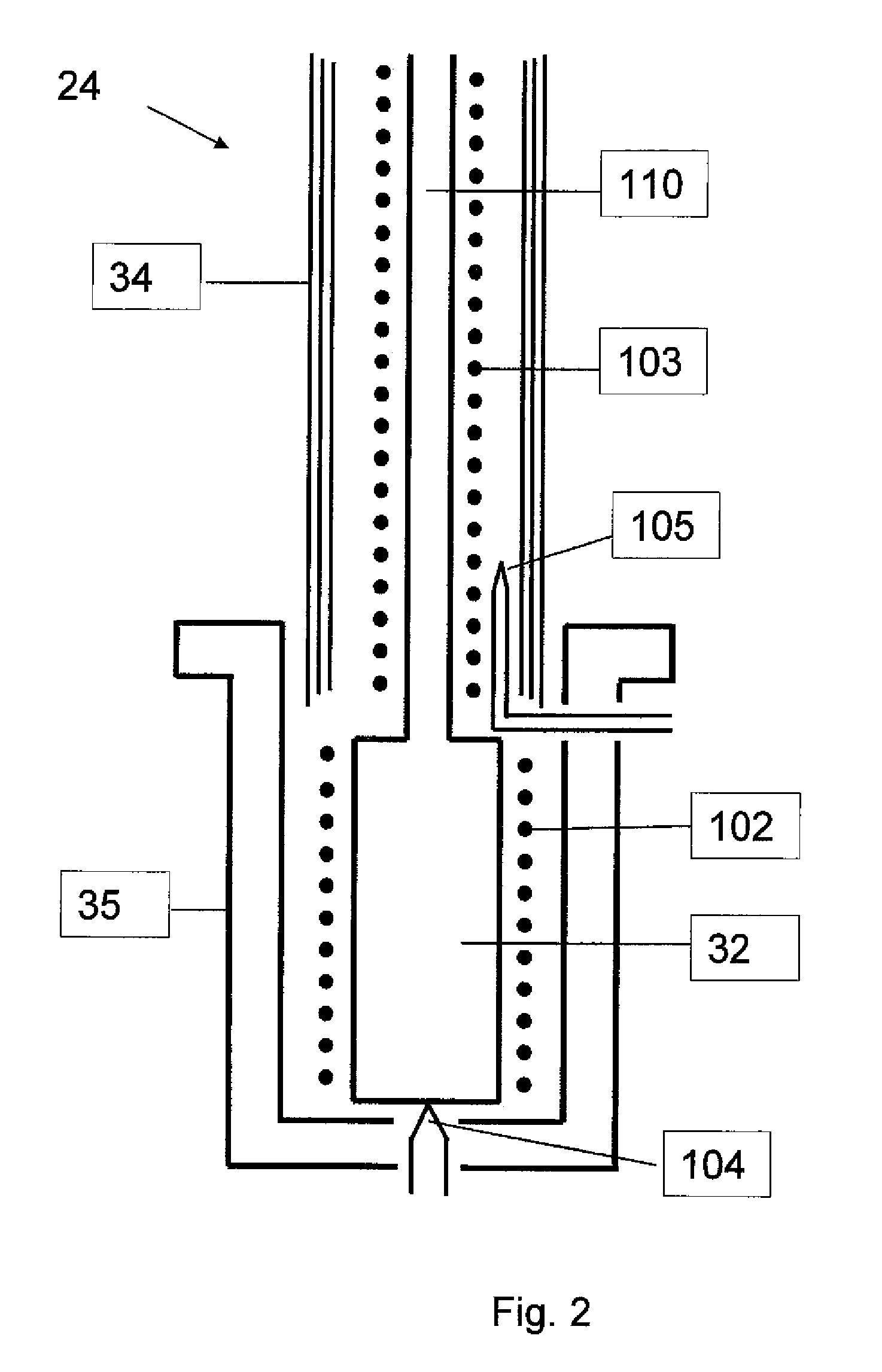
  • Methodology for forming pnictide compositions suitable for use in microelectronic devices
  • Methodology for forming pnictide compositions suitable for use in microelectronic devices
  • Methodology for forming pnictide compositions suitable for use in microelectronic devices

Examples


example 1

Growth of Zn3P2 Thin Films from a Zn3P2 Compound Source and Supplemental Zn Source

[0124]An undoped GaAs(001) growth substrate was first etched in H2SO4:H2O2:H2O (4:1:100 vol) for two minutes followed by an HCl:H2O (1:3) etch for an additional two minutes, then rinsed in DI water for 20 to 30 seconds and nitrogen blow-dried. The substrate was attached to a molybdenum sample holder using copper-beryllium clips. A small area of lithographic mask was applied to the surface of the wafer which could later be removed by acetone after growth for determining film thickness. The substrate holder was then immediately placed under vacuum.

[0125]Within a molecular beam epitaxial growth chamber, the sample was first annealed at 300° C. for 30 minutes to 1 hour to outgas any water or carbon contaminents followed by a higher temperature anneal at 450° C. which facilitated reconstruction of the GaAs surface. The substrate was allowed to cool to 200° C., during which time both the Zn3P2 compound sourc...

example 2

Growth of ZnxPy Thin Films from a Zn3P2 Compound Source and Supplemental Zn Source

[0126]Several experiments were conducted in the exact same manner as outlined in Example 1 except that the temperature of the zinc metal effusion cell was set to 320° C., 325° C., 330° C., 335° C., 340° C., 350° C., and 360° C., respectively. Data is shown in FIGS. 6A and 6B. FIG. 6a shows the influence of additional zinc source flux on growth rate of zinc phosphide thin films. A clear increase in growth rate was observed as the temperature of the zinc source was increased past 330° C. Films grown with the zinc source below 330° C. were found to be amorphous in nature. Crystalline Zn3P2 films were obtained for zinc source temperatures at or greater than 300° C. Film thicknesses were measured by profilometry. FIG. 6b shows the influence of additional zinc metal flux on the stoichiometry of grown films. Films grown without the additional zinc source were found to be phosphorus rich. A perfect Zn3P2 stoic...

example 3

Control of P4 / P2 Ratio in the Flux Via Temperature Control in the Thermal Cracking Zone Using a Zn3P2 Compound Source

[0127]In a molecular beam epitaxial chamber, the source temperature for sublimation of Zn3P2 was heated at a rate of 12° C. per minute to 350° C. and held at that temperature. The cracker temperature in the decomposition zone was adjusted between 400° C. and 1000° C. and the partial pressures of tetramer and dimer species were determined in situ using a quadrapole mass-spectrometer located within the effusion cell beam path. Data is shown in FIGS. 7a and 7b.

[0128]FIG. 7a shows beam equivalent pressure (BEP) of the Zn3P2 compound source effusion cell as a function of source temperature for a thermal treatment decomposition temperature of 1000° C. BEP was determined using a standard nude ionization gauge located within the effusion cell beam path and is uncorrected for ionization sensitivities of Zn and P2 vapor species. Chamber background pressures (open circles) were...


PUM

PropertyMeasurementUnit
temperaturesaaaaaaaaaa
temperatureaaaaaaaaaa
temperaturesaaaaaaaaaa

Abstract

The present invention provides methods for making pnictide compositions, particularly photoactive and / or semiconductive pnictides. In many embodiments, these compositions are in the form of thin films grown on a wide range of suitable substrates to be incorporated into a wide range of microelectronic devices, including photovoltaic devices, photodetectors, light emitting diodes, betavoltaic devices, thermoelectric devices, transistors, other optoelectronic devices, and the like. As an overview, the present invention prepares these compositions from suitable source compounds in which a vapor flux is derived from a source compound in a first processing zone, the vapor flux is treated in a second processing zone distinct from the first processing zone, and then the treated vapor flux, optionally in combination with one or more other ingredients, is used to grow pnictide films on a suitable substrate.

Description

PRIORITY[0001]This application claims the benefit from International No. PCT / US2012 / 024670, which was granted an International filing date of Feb. 10, 2012, which in turn claims priority from United States Provisional patent application having Ser. No. 61 / 441,997, filed on Feb. 11, 2011, by Kimball et al. and entitled METHODOLGY FOR FORMING PNICTIDE COMPOSITIONS SUITABLE FOR USE IN MICROELECTRONIC DEVICES, which applications are incorporated herein by reference in their entireties.FIELD OF THE INVENTION[0002]The present invention relates to methods of forming pnictide compositions suitable for use in microelectronic devices. More specifically, the vapor flux used to form the pnictide compositions is derived from pnictide source compounds, and the vapor flux is at least partially decomposed for use to grow pnictide films. The generation of the vapor flux and the decomposition of the flux occur at least partially in separate processing zones.BACKGROUND OF THE INVENTION[0003]Zinc phosp...

Claims


Application Information

Patent Timeline
Patent Type & Authority Patents(United States)
IPC IPC(8): H01L21/00C30B23/02C30B29/40H01L21/02H01L31/032H01L31/0392H01L31/068H01L31/075H01L31/18
CPCH01L31/18C30B23/02C30B29/40H01L21/02395H01L21/02409H01L21/02538H01L21/02568H01L21/02573H01L21/0262H01L21/02631H01L31/0321H01L31/0392H01L31/068H01L31/075Y02E10/547Y02E10/548
Inventor KIMBALL, GREGORY M.BOSCO, JEFFREY P.ATWATER, HARRY A.LEWIS, NATHAN S.DEGROOT, MARTY W.STEVENS, JAMES C.
Owner DOW GLOBAL TECH LLC
Learn More