Betavoltaic apparatus and method

a betavoltaic and battery technology, applied in the field of betavoltaics, can solve the problems of significant increase in leakage current, increase in packaging volume, and decrease in the overall power density of the battery, and achieve high fuel-fill efficiency, high voltage and power density, and maximize efficiency

Active Publication Date: 2014-10-21
CORNELL UNIVERSITY
View PDF7 Cites 5 Cited by
  • Summary
  • Abstract
  • Description
  • Claims
  • Application Information

AI Technical Summary

Benefits of technology

[0012]A general embodiment of the invention is directed to a ‘very thin’ betavoltaic cell, with top and bottom metallization. In an exemplary aspect, SiC wafers are thinned to thicknesses comparable to electron absorption depths, for maximizing efficiency. It should be noted, however, that any semiconducting material that can sustain a depletion layer (including, e.g., but not limited to Si, GaN, InN, BN) may be used as a substrate material for the thinned-down betavoltaic device. The embodied architecture allows the radioisotope to be integrated in a planar way. According to an aspect, multiple very thin betavoltaic cells can be cascaded in parallel or series to generate higher voltage and power density such that once cascaded, very high fuel-fill efficiencies are possible.
[0016]A general embodiment of the invention is directed to a process for fabricating a very thin betavoltaic cell and, additionally, for cascading two or more very thin betavoltaic cells, resulting in cells that generate higher voltage and power density.

Problems solved by technology

Higher energy β-emitting isotopes such as 137Cs and 90Sr have higher fuel power densities due to their high energy, but because these fuels emit very high electrons and significant x-ray flux, packaging volume increases significantly as shielding is needed, which decreases the overall power density of the battery.
Different techniques of improving the FFF of a betavoltaic battery by patterning and etching of its active device layers have been previously reported; however, in all reported cases, the leakage currents were significantly increased due to the damage to the semiconductor materials in the etching process.
Hence very low conversion efficiencies have been experimentally reported, and overall power density has seen little or no improvement in actual devices made so far.
Therefore, conventional planar betavoltaics may waste over 90% of their volume.
Furthermore, in a planar device 50% of all of the electrons irradiated away from substrate are wasted.

Method used


Image

  • Betavoltaic apparatus and method
  • Betavoltaic apparatus and method
  • Betavoltaic apparatus and method

Examples


Embodiment Construction

[0028]Reference will now be made in detail to the present exemplary embodiments of the invention, non-limiting examples of which are illustrated in the accompanying drawings. Wherever possible, the same reference numbers will be used throughout the drawings to refer to the same or like parts.

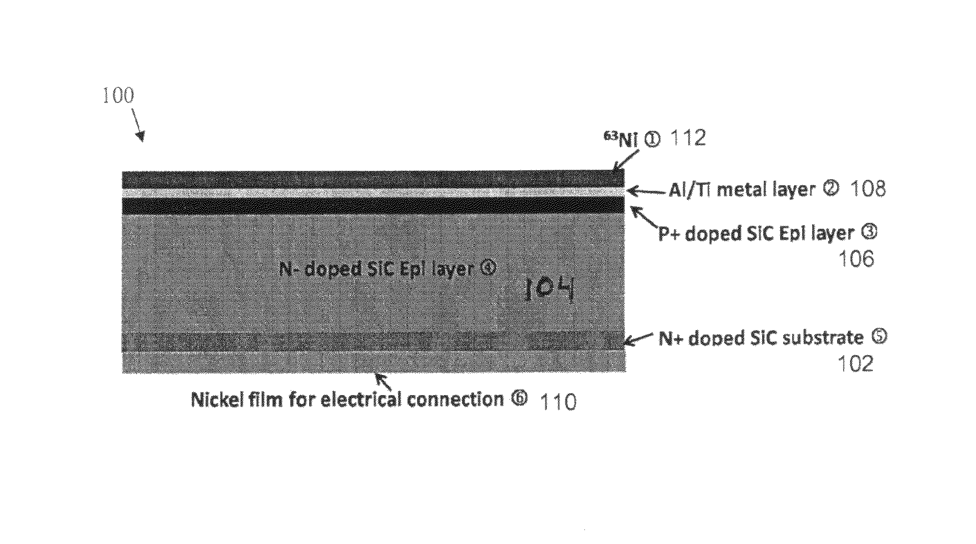
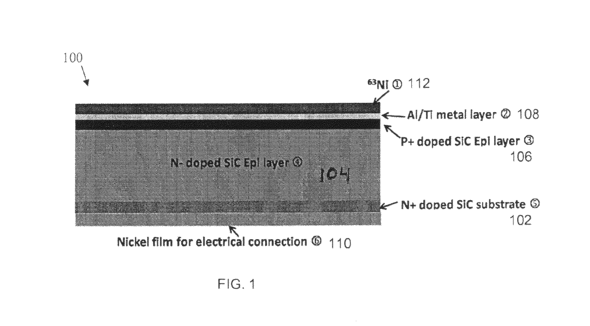
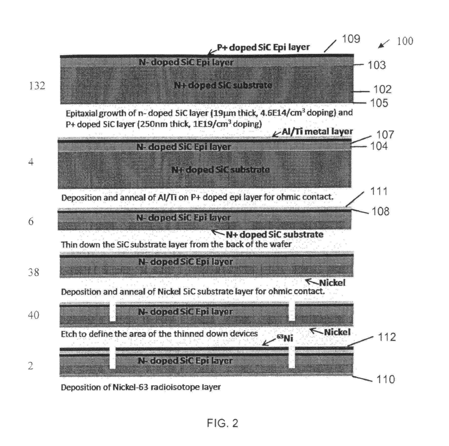
[0029]FIG. 1 schematically illustrates a betavoltaic device 100 according to a non-limiting, exemplary embodiment of the invention. Betavoltaic device 100 includes an N+ doped silicon carbide (SiC) substrate 102 having a top surface 103 and a bottom surface 105. The device 100 further includes an N− doped SiC epitaxial layer 104 having a top surface 107, disposed immediately adjacent the top surface 103 of the SiC substrate; a P+ doped SiC epitaxial layer 106 having a top surface 109, disposed immediately adjacent the top surface 107 of the N− doped SiC epitaxial layer; an aluminum / titanium ohmic conductive layer 108 having a top surface 111, disposed immediately adjacent the top surface 109 of ...


PUM


Abstract

An exemplary thinned-down betavoltaic device includes an N+ doped silicon carbide (SiC) substrate having a thickness between about 3 to 50 microns, an electrically conductive layer disposed immediately adjacent the bottom surface of the SiC substrate; an N− doped SiC epitaxial layer disposed immediately adjacent the top surface of the SiC substrate, a P+ doped SiC epitaxial layer disposed immediately adjacent the top surface of the N− doped SiC epitaxial layer, an ohmic conductive layer disposed immediately adjacent the top surface of the P+ doped SiC epitaxial layer, and a radioisotope layer disposed immediately adjacent the top surface of the ohmic conductive layer. The radioisotope layer can be 63Ni, 147Pm, or 3H. Devices can be stacked in parallel or series. Methods of making the devices are disclosed.

Description

CROSS-REFERENCE TO RELATED APPLICATIONS[0001]This application claims priority to U.S. provisional Patent Application Ser. No. 61 / 262,672 filed on Nov. 19, 2009, the content of which is incorporated herein by reference in its entirety.FEDERALLY SPONSORED RESEARCH[0002]This invention was made with government support under Project ID Nos. W31P4Q-04-1-R002 and ND N66001-07-1-2019 awarded by DARPA. The United States government has certain rights in the invention.BACKGROUND OF THE INVENTION[0003]1. Field of the Invention[0004]Embodiments of the present invention relate generally to the field of betavoltaics; more particularly to a semiconductor-betavoltaic apparatus, method of fabrication, and applications thereof; and, more particularly to a silicon carbide (SiC) betavoltaic apparatus, method of fabrication, and applications thereof.[0005]2. Technical Background[0006]A betavoltaic battery consists of a semiconductor diode that is exposed to electrons emitted from a beta-emitting radioiso...

Claims


Application Information

Patent Timeline
Patent Type & Authority Patents(United States)
IPC IPC(8): H01L29/15G21H1/06
CPCG21H1/06
Inventor LAL, AMITTIN, STEVEN
Owner CORNELL UNIVERSITY
Why Eureka
Try Eureka