Semiconductor device test method and apparatus, and semiconductor device

a technology of semiconductor devices and test methods, applied in the field of semiconductor devices, can solve the problem of insufficient increase of achieve the effect of increasing the dielectric strength of the devi

Active Publication Date: 2011-12-08
MITSUBISHI ELECTRIC CORP
View PDF7 Cites 8 Cited by
  • Summary
  • Abstract
  • Description
  • Claims
  • Application Information

AI Technical Summary

Benefits of technology

[0007]The present invention has been made to solve this problem. It is, therefore, an object of the present invention to provide a semiconductor device having a plurality of conductive patterns which have optimum configurations

Problems solved by technology

It has been found, however, that this requirement may prevent the conductive patterns from having an optimum configuration for increasing

Method used


Image

  • Semiconductor device test method and apparatus, and semiconductor device
  • Semiconductor device test method and apparatus, and semiconductor device
  • Semiconductor device test method and apparatus, and semiconductor device

Examples


first embodiment

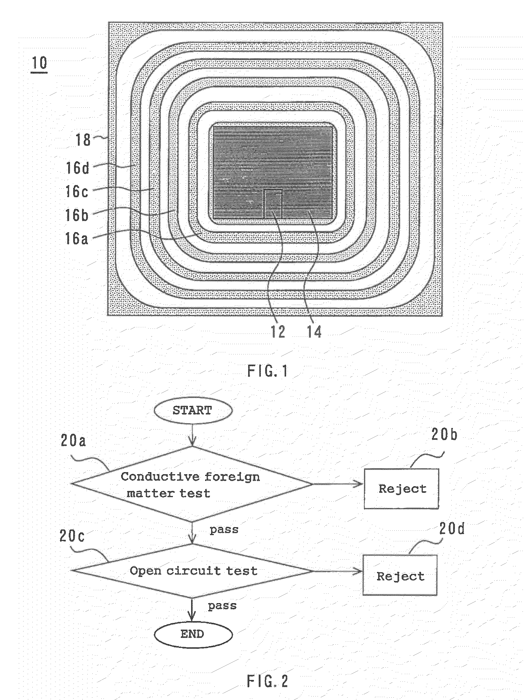
[0029]There will now be described a method of testing a semiconductor device in accordance with a first embodiment of the present invention. FIG. 1 is a plan view of a semiconductor device 10. This semiconductor device 10 is an IGBT formed on a semiconductor substrate. A gate electrode 12 and an emitter electrode 14 are formed at the center of the semiconductor device 10. Conductive patterns 16a, 16b, 16c, and 16d are formed to encircle the gate electrode 12 and the emitter electrode 14. The conductive patters 16a, 16b, 16c, and 16d are made of aluminum. They are insulated from one another. A channel stopper electrode 18 is formed to encircle the conductive patterns 16a, 16b, 16c, and 16d.

[0030]FIG. 2 is a flowchart showing the method of testing a semiconductor device in accordance with the first embodiment. The method begins by performing a conductive foreign matter test process (step 20a). This conductive foreign matter test process is used to determine whether any conductive for...

second embodiment

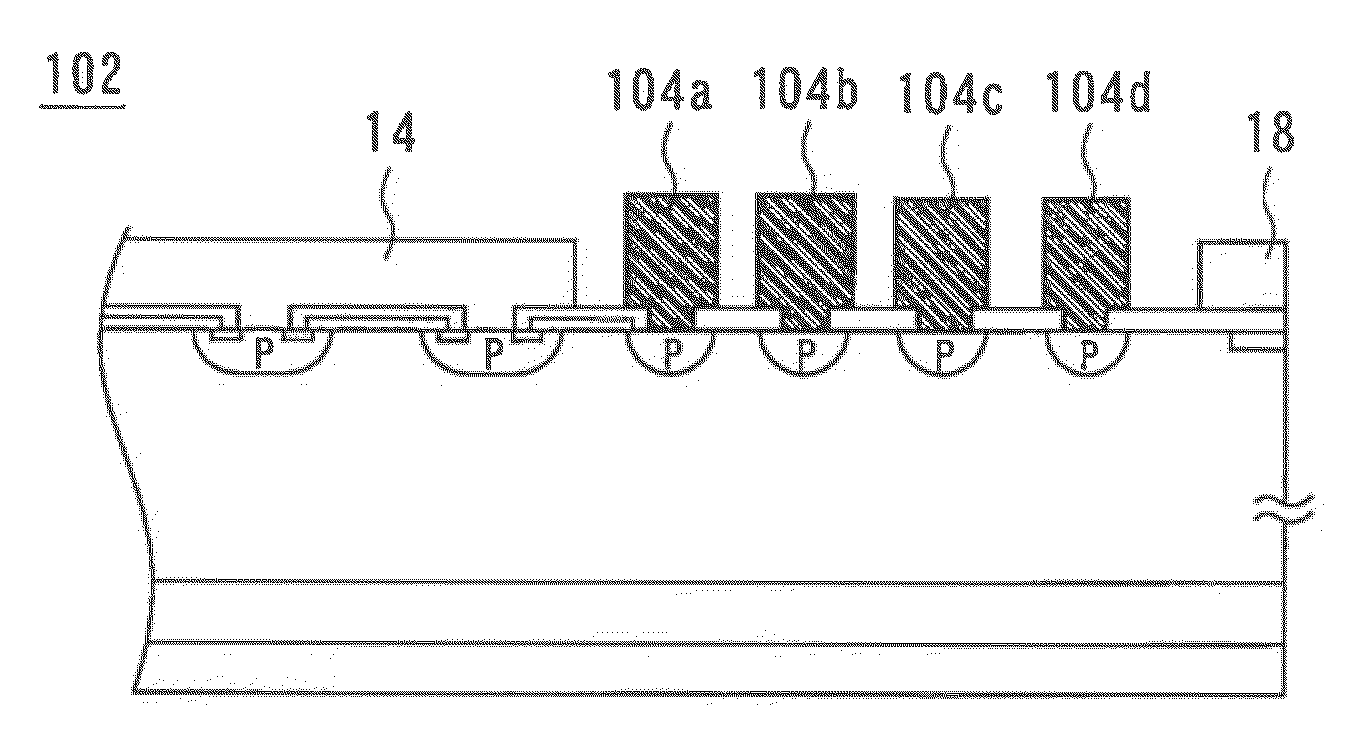
[0046]A semiconductor device in accordance with a second embodiment of the present invention is characterized in that an overcoating film having openings is formed on the conductive patterns. An overcoating film is a high resistance film formed on a conductive pattern or patterns The overcoating film serves to stabilize the dielectric strength of the semiconductor device. FIG. 9 is a cross-sectional view of the semiconductor device of the second embodiment. The semiconductor device, 80, includes an emitter electrode 14 and an overcoating film 82 covering the conductive patterns 16a, 16b, 16c, and 16d and the channel stopper electrode 18. The overcoating film 82 has openings 84a, 84b, 84c, and 84d exposing portions of the top surfaces of the conductive patters 16a, 16b, 16c, and 16d, respectively.

[0047]The semiconductor device 80 thus constructed is subjected to a conductive foreign matter test process and an open circuit test process (which may be hereinafter referred to collectivel...

third embodiment

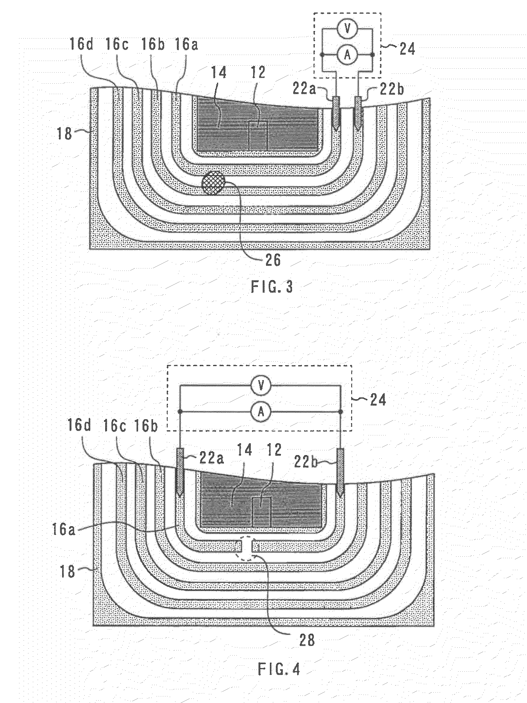
[0049]An apparatus for testing a semiconductor device in accordance with a third embodiment of the present invention is characterized in that its probes are provided with a spring. FIG. 11 is a schematic diagram showing the test apparatus of the third embodiment. The test apparatus, 90, includes a spring 92a and a spring 92b. The springs 92a and 92b are attached to the probes 22a and 22b, respectively, so that the springs 92a and 92b can be expanded and contracted in the direction in which the probes 22a and 22b are pressed against conductive patterns (i.e., in the direction of the arrow in FIG. 11).

[0050]The measurement unit 24 of the test apparatus 90 is adapted to measure the resistance between the probes 22a and 22b by use of an ammeter and a voltmeter. This test apparatus 90 is used to perform test processes such as described above.

[0051]Incidentally, the positions of the top surfaces of the conductive patterns may vary due to variations in the thickness of the conductive patte...


PUM


Abstract

A method of testing a semiconductor device includes a conductive foreign matter test step of measuring the resistance value between the first and second conductive patterns to determine whether conductive foreign matter is present between the first and second conductive patterns, a first open circuit test step of measuring the resistance value between two points on the first conductive pattern to determine whether there is an open circuit in the first conductive pattern, and a second open circuit test step of measuring the resistance value between two points on the second conductive pattern to determine whether there is an open circuit in the second conductive pattern. The measurement of the resistance value in each of the test steps is accomplished by pressing probes vertically against the first conductive pattern or the second conductive pattern or both.

Description

BACKGROUND OF THE INVENTION[0001]1. Field of the Invention[0002]The present invention relates to a semiconductor device having a plurality of conductive patterns and to a method and apparatus for testing the device.[0003]2. Background Art[0004]Some semiconductor devices have a guard ring structure designed to enhance the dielectric strength of the device. The guard ring structure includes a first conductivity type layer and a plurality of annular second conductivity type regions (i.e., guard rings) formed in the first conductivity type layer. Conductive patterns are formed on the guard rings to stabilize the potential of the guard rings. More specifically, each conductive pattern is formed on a respective one of the guard rings. The conductive patterns must be insulated from one another and must be free from open circuits or breaks.[0005]Therefore, the manufacturing process of a semiconductor device includes a test process for determining whether the conductive patterns meet these r...

Claims


Application Information

Patent Timeline
IPC IPC(8): G01R1/067G01R31/26H01L23/48
CPCG01R31/026G01R31/2853H01L2924/0002H01L2924/00G01R31/52G01R31/54G01R27/02G01R31/26
Inventor NARAZAKI, ATSUSHI
Owner MITSUBISHI ELECTRIC CORP
Why Eureka
Try Eureka