

Apparatus for single-molecule detection
a single-molecule, detection apparatus technology, applied in the direction of optical radiation measurement, nuclear engineering, biomass after-treatment, etc., can solve the problems of limited throughput, scale-up, and limited detection number of zmws
- Summary
- Abstract
- Description
- Claims
- Application Information
AI Technical Summary
Problems solved by technology
Method used
Image

Examples
example 1
3.1 Example 1
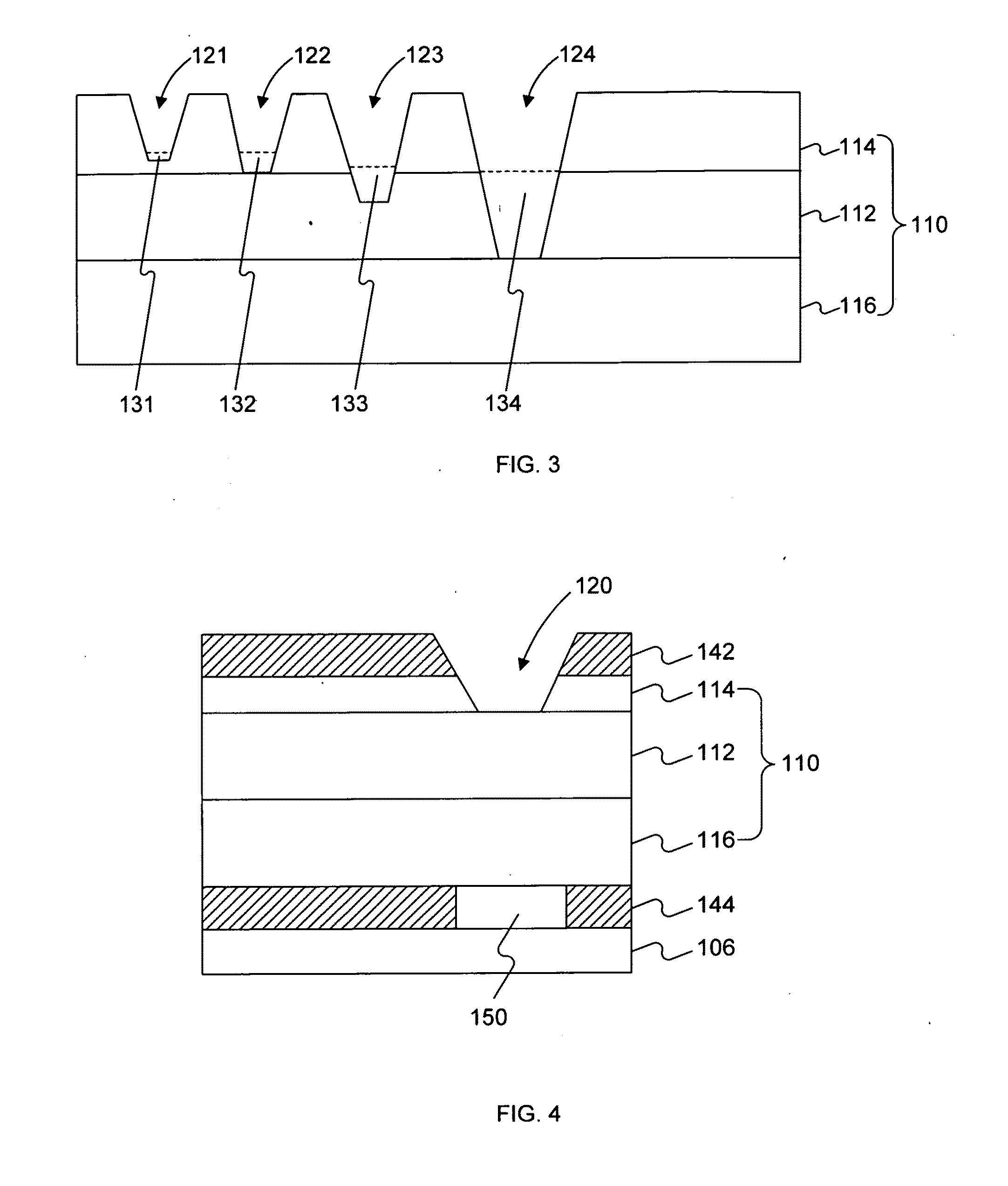
[0157]FIGS. 16A-16D show the computer-simulation results for nanowell 121, 122, 123, and 124 shown in FIG. 3, respectively. In the simulation, a finite-differential-time-domain (FDTD) method was used to compute the electric field distribution of the excitation light propagating along the longitudinal direction of the waveguide and passing by or through the effective excitation zone. The strength of the electric field may represent the intensity of the electromagnetic field of the light in the waveguide. In FIGS. 16A-16D, the strength of the electric field is shown in an arbitrary unit.
[0158]In order to more closely simulate the actual situation, in this simulation, a particle having a diameter of 100 nm was assumed to be near the bottom of the nanowell. The refractive index of the particle was set to be 2.5. The refractive index of the core layer was set to be 2.25, the refractive indices of the upper and lower cladding layers were set to be 1.45, the refractive index o...
example 2
3.2 Example 2
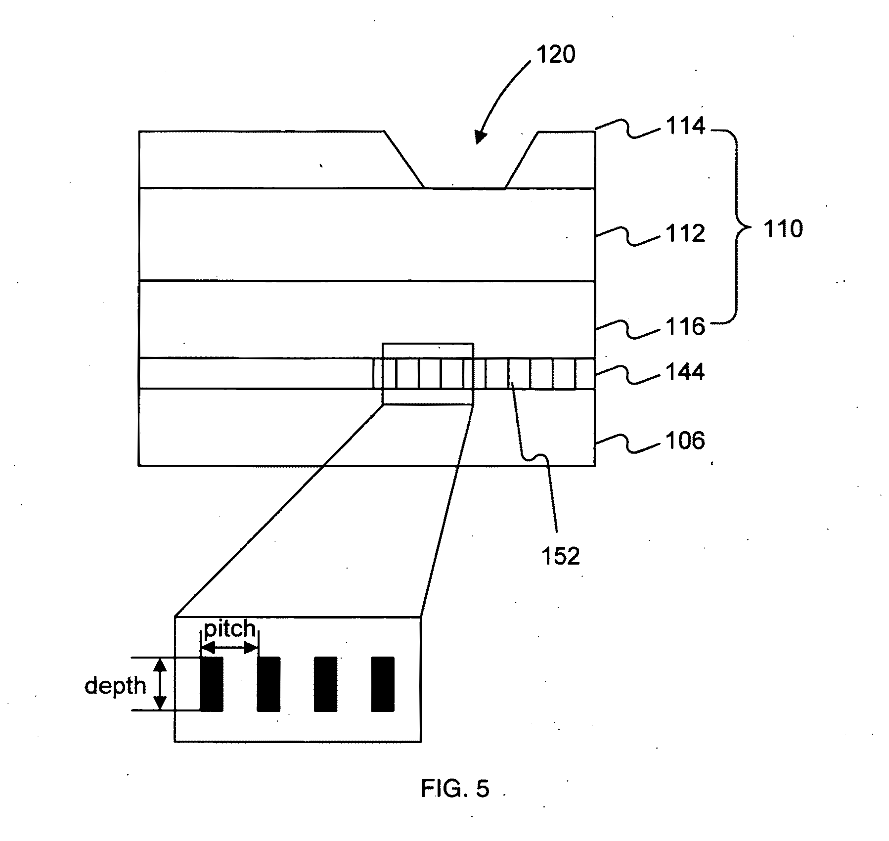
[0159]This example illustrates the simulation results of the transmittances of a TE mode light having a wavelength of 473 nm and TM mode light having a wavelength of 550 nm through a metal pattern as in the structure shown in FIG. 5 as functions of grating period and depth of the metal pattern, respectively.
[0160]FIG. 17A shows the simulated transmittances of the TE mode light through the metal pattern versus the grating period of the metal pattern. Different curves in FIG. 17A represent results computed at different values of metal pattern depth.
[0161]FIG. 17B shows the simulated transmittances of the TM mode light through the metal pattern versus the grating period of the metal pattern. Different curves in FIG. 17B represent results computed at different values of metal pattern depth.
[0162]It is seen from FIG. 17B that, when the grating period of the metal pattern is smaller than 300 nm, the transmittance of the TM mode light is higher than about 30%, which is also mu...
example 3
3.3 Example 3
[0163]This example illustrates calculated transmittances of a TE mode light and a TM mode light through the metal pattern in the structure shown in FIG. 5. In this example, nanostructured metal pattern 152 is made of aluminum and the lower protection layer 144 surrounding the aluminum pattern is made of silicon oxide. The periodicity and depth of the aluminum pattern are 110 nm and 245 nm, respectively. FIGS. 18A and 18B show the transmittances of the TE mode light and the TM mode light as a function of incident angle, respectively. It is seen from FIGS. 18A and 18B that, the transmittance of the TE mode light decreases from about 10−8 to about 10−12 when the absolute value of the incident angle increases from 0 degree to larger than 60 degree, whereas the transmittance of the TM mode light is always higher than 60% within the range of the incident angle from about −60 degree to about 60 degree.
PUM
| Property | Measurement | Unit |
|---|---|---|
| surface roughness | aaaaa | aaaaa |
| diameter | aaaaa | aaaaa |
| diameter | aaaaa | aaaaa |
Abstract
Description
Claims
Application Information