Semiconductor light-emitting device and manufacturing method

Active Publication Date: 2011-12-22
STANLEY ELECTRIC CO LTD
View PDF1 Cites 114 Cited by
  • Summary
  • Abstract
  • Description
  • Claims
  • Application Information

AI Technical Summary

Benefits of technology

[0025]According to the exemplary manufacturing method described above for the semiconductor light-emitting devices, the side slant surface of the reflective material layer used as the reflector can be formed by disposing an uncured reflective material between the frame and both side surfaces of the wavelength converting layer and the transparent material layer. The transparent materi

Problems solved by technology

Accordingly, it may be difficult for the lead frame type light-emitting device 20 to reduce a light-emitting surface.
Additionally, the radial type light-emitting device 30 may emit a wavelength-converted light in a radial fashio

Method used


Image

  • Semiconductor light-emitting device and manufacturing method
  • Semiconductor light-emitting device and manufacturing method
  • Semiconductor light-emitting device and manufacturing method

Examples


first embodiment

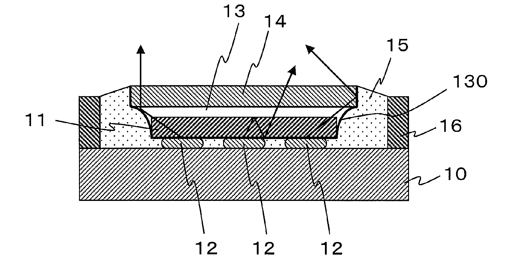
[0086]A reflective material layer 15 can be disposed around an outer side surface of the light-emitting chips 11 that faces a frame 16 and can include a side slant surface 130, which is a boundary between the reflective material layer 15 and the transparent material layer 13 and which wholly surrounds the light-emitting chips 11. The side slant surface 130 can be formed in a substantially linear shape connecting an end of the bottom surface of the wavelength converting layer 14 to a bottom end of the outer side surface of the light-emitting chips 11, and also can be formed in a convex shape in an inward direction of the semiconductor light-emitting device as shown in FIGS. 8a to 8c. In this case, the side slant surface 130 can be formed in a curvature of 5 or less due to the same reason as described above with respect to the

[0087]The reflective material layer 15 can be disposed between the bottom surfaces of the light-emitting chips 11 and a mounting surface of a base board 10 mount...

second embodiment

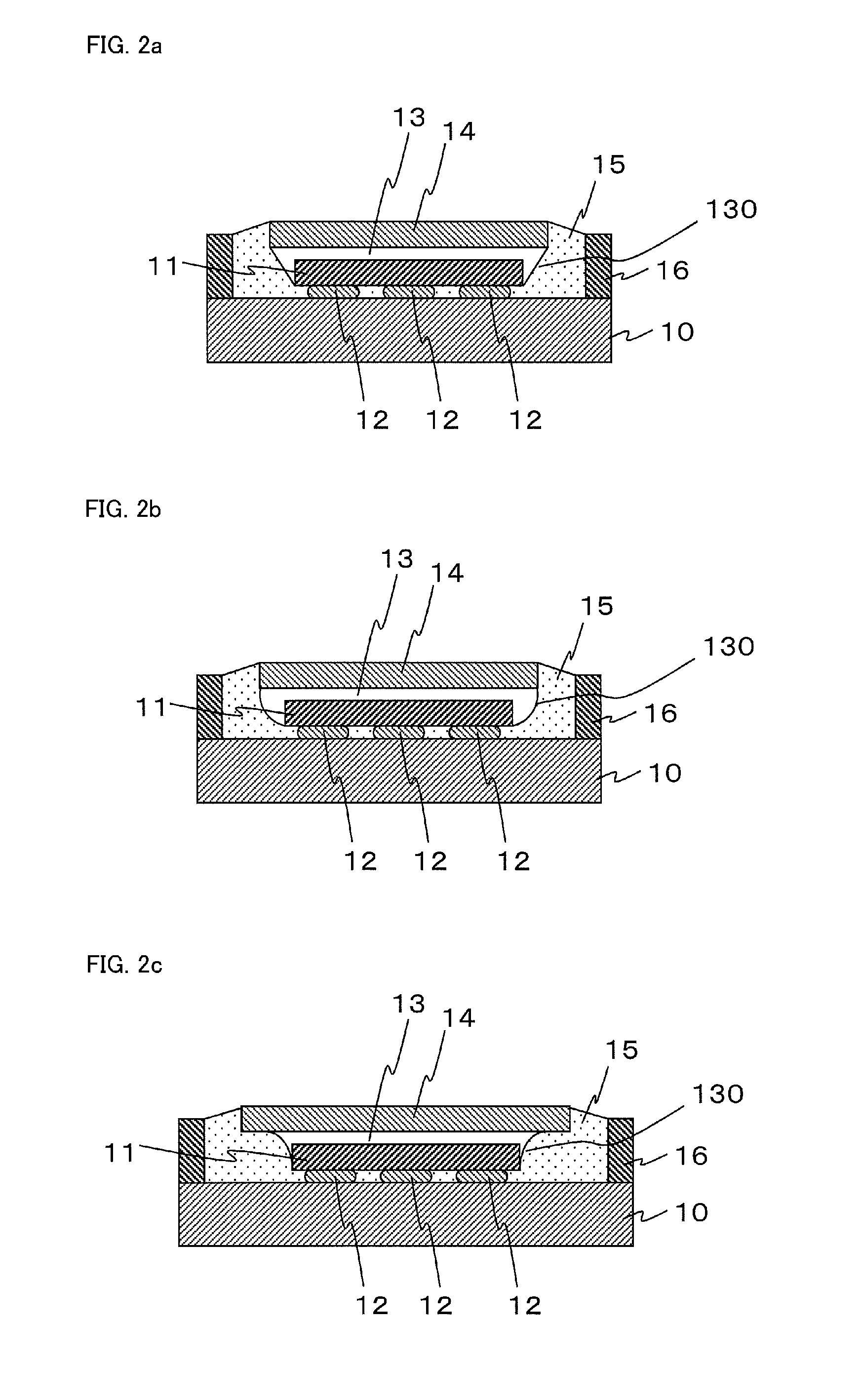
[0095]In addition, because the semiconductor light-emitting device of the second embodiment can prevent a reduction of light intensity between the adjacent light-emitting chips 11 by forming the convex shape 81 in each of the spaces between the adjacent light-emitting chips 11, the disclosed subject matter can provide semiconductor light emitting devices which can reduce a variation of a light intensity on the light-emitting surface.

[0096]FIGS. 9a and 9b are cross-section views depicting exemplary comparative embodiments including a plurality of light-emitting chips of a semiconductor light-emitting device. To compare an optical characteristic of Sample A of the second embodiment shown FIG. 8b, Sample B includes reflective material 15 disposed in a cavity formed of the frame 16 and the base board 10 so as to fill a space surrounding the light-emitting chips 11 and the side surface of the wavelength converting layer 14 and so as to exclude the transparent material layer 13 as shown i...


PUM


Abstract

A semiconductor light-emitting device and a method for manufacturing the same can include a wavelength converting layer located over at least one semiconductor light-emitting chip in order to emit various colored lights including white light. The semiconductor light-emitting device can include a base board, a frame located on the base board, the chip mounted on the base board, a transparent material layer located between the wavelength converting layer and a side surface of the chip so as to extend toward the wavelength converting layer, and a reflective material layer disposed at least between the frame and both side surfaces of the wavelength converting layer and the transparent material layer. The semiconductor light-emitting device can be configured to improve light-emitting efficiency of the chip by using the reflective material layer as a reflector, and therefore can emit a wavelength-converted light having a high light-emitting efficiency from a small light-emitting surface.

Description

[0001]This application claims the priority benefit under 35 U.S.C. §119 of Japanese Patent Application No. 2010-137365 filed on Jun. 16, 2010, which is hereby incorporated in its entirety by reference.BACKGROUND[0002]1. Field[0003]The presently disclosed subject matter relates to semiconductor light-emitting devices in which light emitted from a semiconductor light-emitting chip is wavelength-converted by a wavelength-converting layer, and to manufacturing methods for the same. More particularly, the disclosed subject matter relates to semiconductor light-emitting devices for a vehicle light and the like, which can emit light having a high light-emitting efficiency from a small light-emitting surface, and to methods of manufacturing such devices.[0004]2. Description of the Related Art[0005]Semiconductor light-emitting devices, in which a part of the light emitted from a semiconductor light-emitting chip is converted into light having a different wavelength by a phosphor and in which...

Claims


Application Information

Patent Timeline
IPC IPC(8): H01L33/08H01L33/60H01L33/50
CPCH01L33/46H01L33/502H01L2224/73253H01L33/60H01L2933/0041H01L33/507
Inventor ITO, KOSABUROSEKO, TOSHIHIROUENO, KAZUHIKOOWADA, SOJI
Owner STANLEY ELECTRIC CO LTD
Why Eureka
Try Eureka