Laterally double diffused metal oxide semiconductor transistor having a reduced surface field structure and method therefor

a metal oxide semiconductor and surface field technology, applied in the field of semiconductors, can solve the problems of limiting the break-down of the buried layer itsel

Active Publication Date: 2011-12-22
NXP USA INC
View PDF4 Cites 38 Cited by
  • Summary
  • Abstract
  • Description
  • Claims
  • Application Information

AI Technical Summary

Problems solved by technology

However, the buried layer itself can become break-down limiting.

Method used


Image

  • Laterally double diffused metal oxide semiconductor transistor having a reduced surface field structure and method therefor
  • Laterally double diffused metal oxide semiconductor transistor having a reduced surface field structure and method therefor
  • Laterally double diffused metal oxide semiconductor transistor having a reduced surface field structure and method therefor

Examples


Embodiment Construction

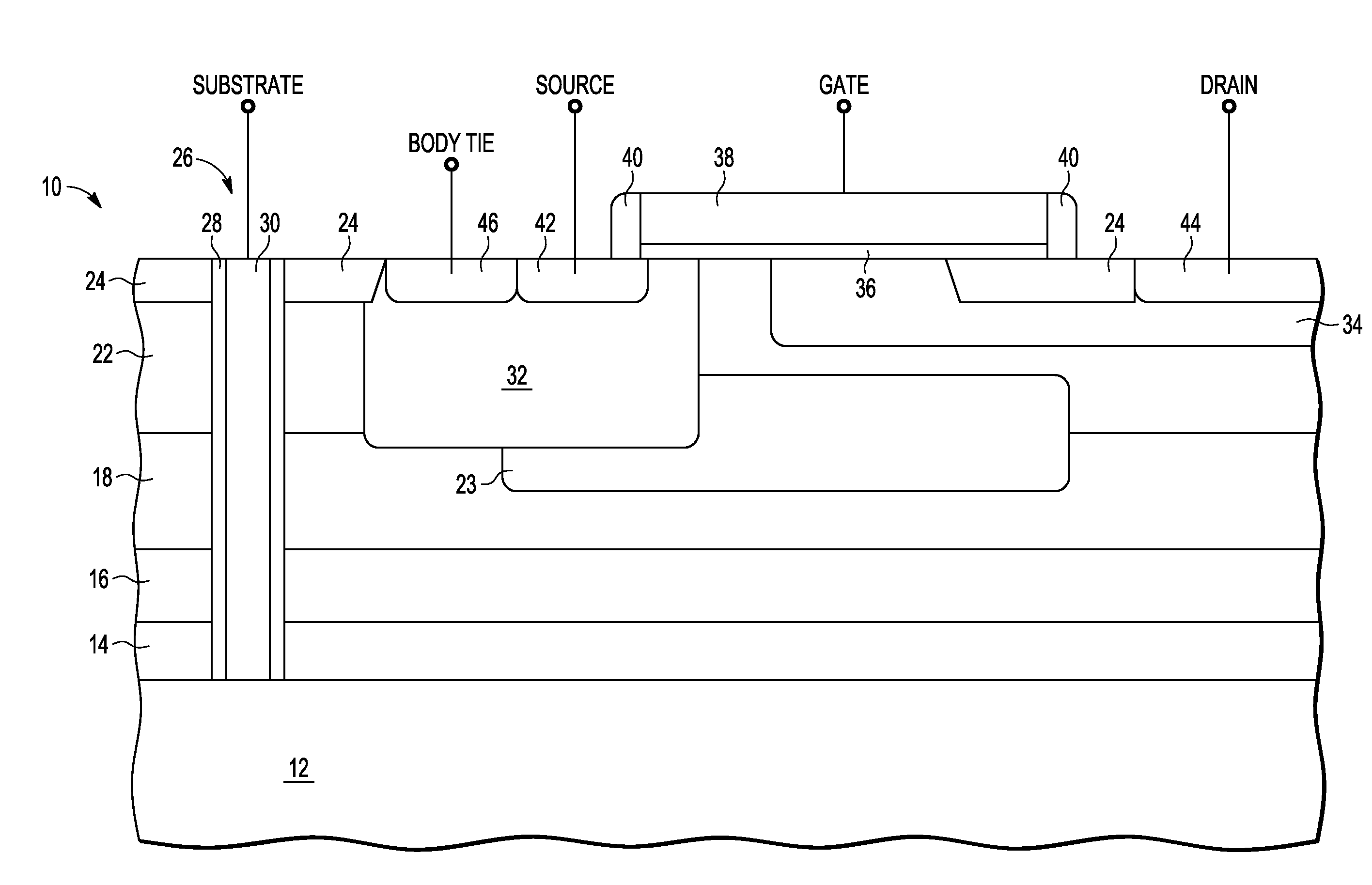
[0012]Generally, there is provided, a P-type LDMOS transistor that is isolated using a buried oxide layer and a deep trench. The deep trench may be filled with polysilicon in one embodiment. Also a lightly doped N-type RESURF region is connected to the source region via a N-type well region. The RESURF region extends to, but not completely under the drain region leaving a gap, or opening, under the drain region. The opening under the drain allows the drain potential to spread over the full depth of the epitaxial layer on top of the buried oxide (BOX) achieving a double RESURF action with the RESURF layer being depleted from P-regions situated above and below. The P-type LDMOS transistor with double RESURF action is realized using P-type epitaxially grown layers. The P-type epitaxially grown layers are typically only optimized for N-type LDMOS transistors leaving the P-type LDMOS in single RESURF configuration for an N-type buried layer. There is provided herein a semiconductor devic...


PUM


Abstract

An LDMOS transistor includes a substrate of semiconductor material, an insulator layer overlying the substrate, a semiconductor layer overlying the insulator layer, a RESURF region, and a gate. The semiconductor layer includes a first conductivity type well region, a second conductivity type source region in contact with the first conductivity type well region, a second conductivity type drain region. The RESURF region includes at least one first conductivity type material portion, and at least one portion of the at least one first conductivity type material portion electrically coupled to the first conductivity type well region. A semiconductor material having a second conductivity type is located below the RESURF region. The second conductivity type semiconductor material is also located over a part of the RESURF region. The gate is located over the first conductivity type well region and over the RESURF region.

Description

BACKGROUND[0001]1. Field[0002]This disclosure relates generally to semiconductors, and more specifically, to a laterally double diffused metal oxide semiconductor (LDMOS) transistor having a reduced surface field structure and method therefor.[0003]2. Related Art[0004]Laterally double diffused metal oxide semiconductor (LDMOS) transistors are used in mixed signal and analog circuits for high power switching. Optimization characteristics such as on resistance (Ron), break-down voltage (BVDSS), and safe operating area (SOA) often conflict. Also, depending on the needs of the particular application, good isolation and high side capabilities may be desirable or necessary. To have high side capability means that a transistor can have all of its terminals coupled to a high potential relative to the substrate, such as when a load is connected to the source of the LDMOS transistor with the drain connected to the supply voltage. Ideally, the performance of a high side capable device does not...

Claims


Application Information

Patent Timeline
Patent Type & Authority Applications(United States)
IPC IPC(8): H01L29/78H01L21/336
CPCH01L29/0634H01L29/0653H01L29/0878H01L29/7816H01L29/66689H01L29/7824H01L29/063H01L29/1095
Inventor GROTE, BERNHARD H.KHAN, TAHIR A.KHEMKA, VISHNU K.ZHU, RONGHUA
Owner NXP USA INC
Why Eureka
Try Eureka