Power Semiconductor Device and Power Conversion Device

a technology of power semiconductor and power semiconductor elements, which is applied in the direction of printed circuit board receptacles, electrical apparatus construction details, electrical apparatus casings/cabinets/drawers, etc., can solve the problems of power semiconductor elements being damaged, gap between molds appearing,

Active Publication Date: 2011-12-22
HITACHI ASTEMO LTD
View PDF13 Cites 104 Cited by
  • Summary
  • Abstract
  • Description
  • Claims
  • Application Information

AI Technical Summary

Benefits of technology

[0025]According to the present invention, the power semiconductor elements will be prevented from being damaged in the manufacturing process of power modules.

Problems solved by technology

However, in the state where the positive electrode-side terminal and the negative electrode-side terminal are laminated as stated in Patent Literature 1 described above, the laminated area is different from other terminals in thickness, and thus over stress on the connection sections between the power semiconductor elements and the terminals and a gap between the molds may occur when clamping.
The over stress on the connection section causes the power semiconductor elements to be damaged.

Method used


Image

  • Power Semiconductor Device and Power Conversion Device
  • Power Semiconductor Device and Power Conversion Device
  • Power Semiconductor Device and Power Conversion Device

Examples


Embodiment Construction

[0067]In the embodiments stated below, in addition to the problems and the advantageous effects stated as problems to be solved by the invention and advantageous effects of the invention respectively, problems are solved and advantageous effects are achieved so as to make a desired product. These will be explained in the following embodiments.

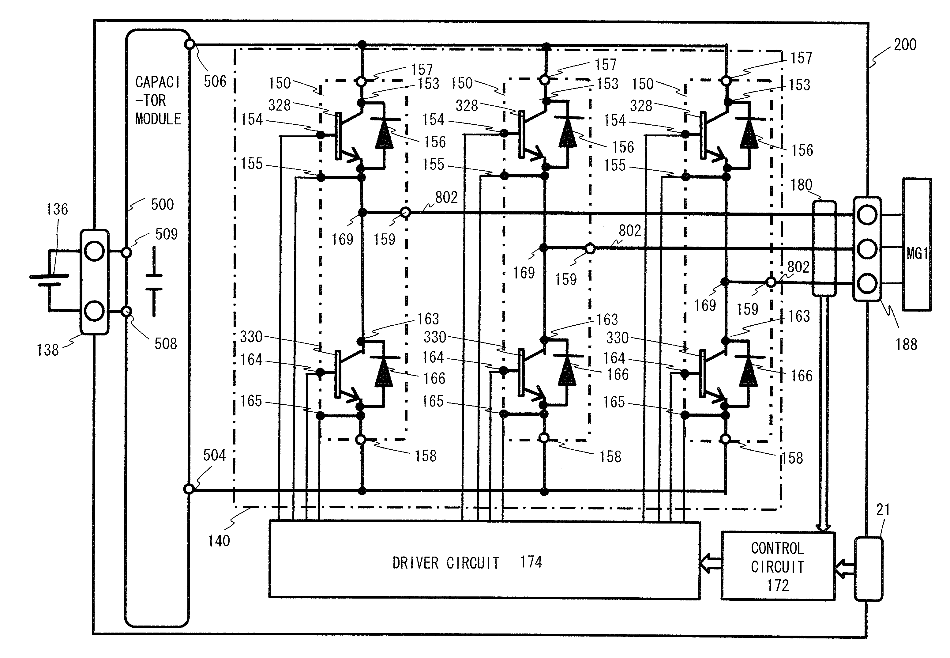
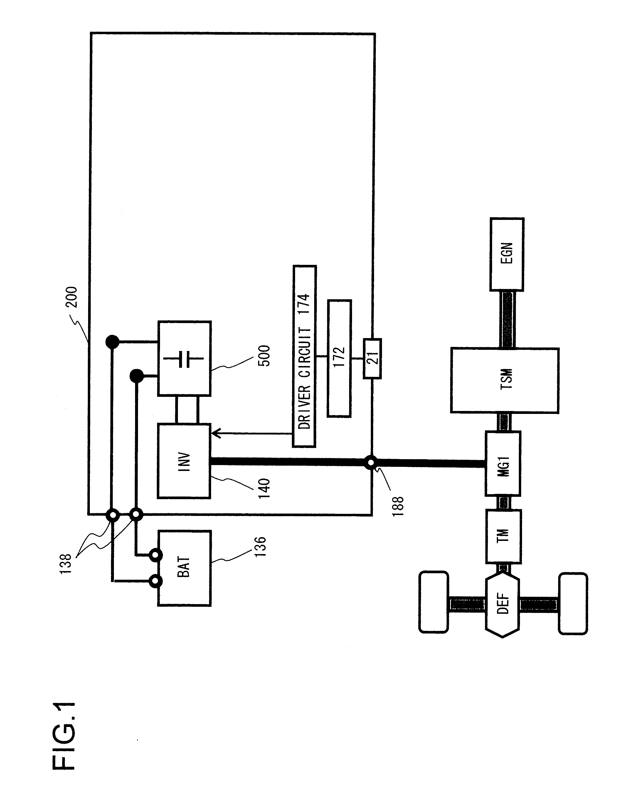
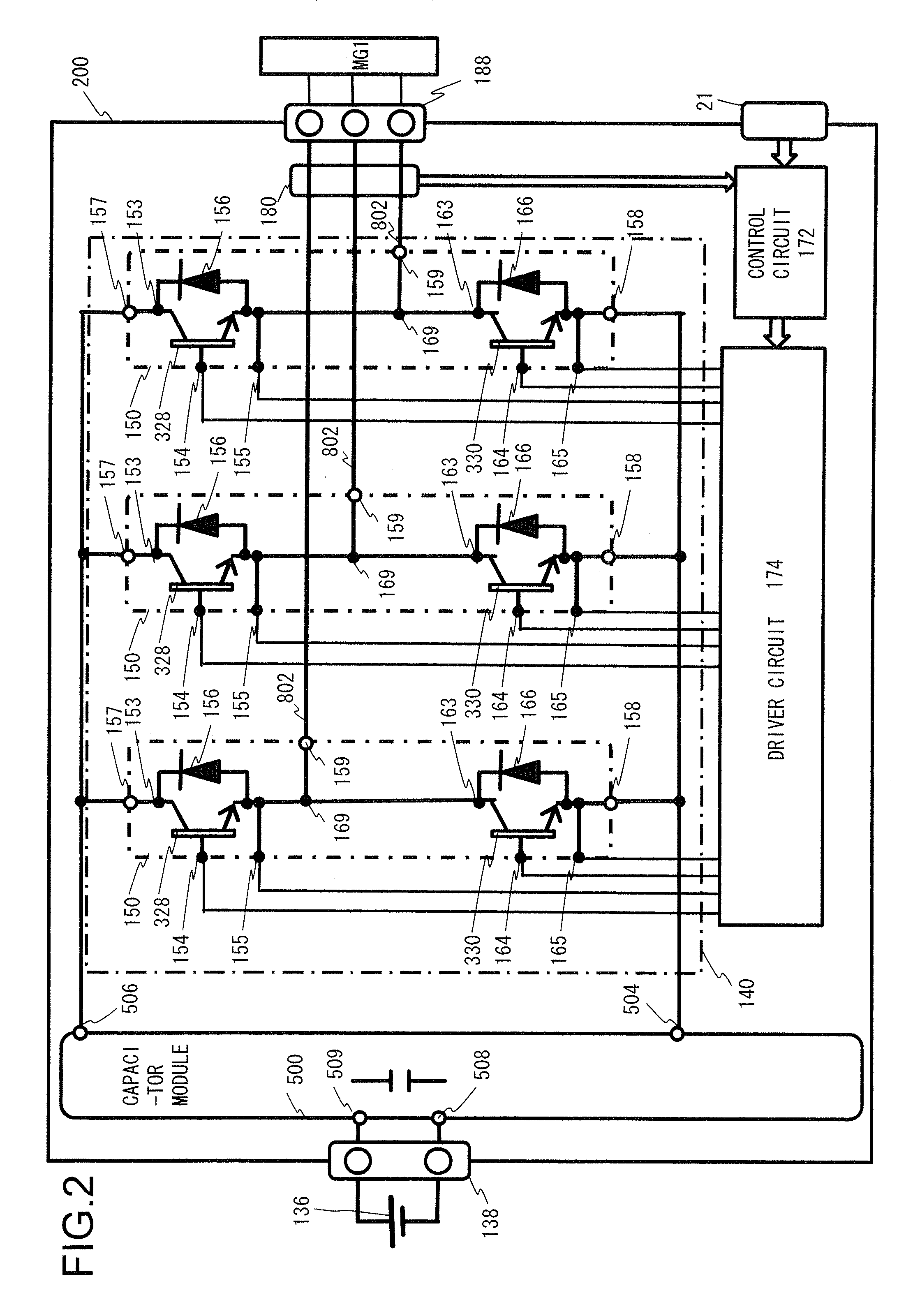
[0068]An embodiment of the present invention will now be explained with reference to the drawings. FIG. 1 is a diagram showing control blocks of a hybrid electric vehicle (hereinafter referred to as “HEV”). An engine EGN and a motor generator MG1 generate torque for driving a vehicle. In addition, the motor generator MG1 has a function not only to generate rotational torque but also to convert mechanical energy applied from outside to the motor generator MG 1 into electric power.

[0069]The motor generator MG 1 is, for example, a synchronous machine or an induction machine, and, as described above, works as a motor or an electric generator depend...


PUM


Abstract

A power semiconductor device includes a plurality of power semiconductor elements constituting upper and lower arms of an inverter circuit, a first sealing member sealing the plurality of power semiconductor elements, a positive electrode-side terminal and a negative electrode-side terminal each connected with any of the plurality of power semiconductor elements and protruding from the first sealing member, a second sealing member sealing at least a part of the positive electrode-side terminal and at least a part of the negative electrode-side terminal, and a case in which the power semiconductor elements sealed with the first sealing member are housed.

Description

INCORPORATION BY REFERENCE[0001]The disclosure of the following priority application is herein incorporated by reference: Japanese Patent Application No. 2010-140723 (filed on Jun. 21, 2010)BACKGROUND OF THE INVENTION[0002]1. Field of the Invention[0003]The present invention relates to a power semiconductor device including power semiconductor elements which perform switching operations to convert direct-current (DC) power to alternating-current (AC) power or AC power to DC power, and relates to a power conversion device using the power semiconductor device.[0004]2. Description of Related Art[0005]A power conversion unit includes a function to convert DC power supplied from a DC power supply into AC power to be supplied to AC electrical load such as a rotating electrical machine or a function to convert AC power generated by a rotating electrical machine into DC power to be supplied to a DC power supply. To serve such conversion function, the power conversion unit includes a power s...

Claims


Application Information

Patent Timeline
Patent Type & Authority Applications(United States)
IPC IPC(8): H05K7/20H01L23/48
CPCH01L2924/1203H01L2924/13055H01L2924/1305H01L2924/1306H01L2924/3025H01L2924/30107H01L2224/8384H01L2224/73265H01L2224/73221H01L2224/73215H01L2224/48247H01L2224/33181H01L2224/32245H01L2224/29139H01L2224/291H01L2924/13091H05K7/20927H01L23/3107H01L23/473H01L23/49562H01L23/49575H01L21/565H01L24/29H01L24/32H01L24/33H01L24/34H01L24/48H01L24/73H01L2924/014H01L2924/00012H01L2924/00H01L2924/351H01L2924/181H01L2224/40137H01L24/40H01L2924/00014H01L2224/83801H01L25/112H01L2224/06181H01L2224/32225H01L2224/0603H05K7/14322H01L2224/45099H01L2224/45015H01L2924/207H01L2224/37099H01L2224/37599H01L2224/84H01L2924/013H01L24/36H05K7/1432H02M7/537H05K5/0247H05K7/20845H05K7/2089
Inventor SUWA, TOKIHITOKANEKO, YUJIROTAKAGI, YUSUKEFUJINO, SHINICHISHIMURA, TAKAHIRO
Owner HITACHI ASTEMO LTD
Why Eureka
Try Eureka