Light emitting screen and method of fabricating the light emitting screen

Inactive Publication Date: 2012-01-12
CANON KK
View PDF0 Cites 3 Cited by
  • Summary
  • Abstract
  • Description
  • Claims
  • Application Information

AI Technical Summary

Benefits of technology

[0009]The present invention can suppress discharge in the peripheral region of th

Problems solved by technology

Unfortunately, the distance between the phosphor surface and the electron-emitting device is about 1 to 2 mm, and thus an intense electric field is formed.
The intense electric field often causes discharge.
Unfortunately, the present inventors have made zealous studies paying attention to the structure disclosed in Japanese Patent Application Laid-Open

Method used


Image

  • Light emitting screen and method of fabricating the light emitting screen
  • Light emitting screen and method of fabricating the light emitting screen
  • Light emitting screen and method of fabricating the light emitting screen

Examples


first embodiment

[0019]FIG. 3 is a partially broken perspective view illustrating a basic configuration of an image display apparatus 41 according to a first embodiment of the present invention. The image display apparatus 41 has a rear plate having a plurality of surface-conduction electron-emitting devices 25 arranged in a two-dimensional lattice pattern and a face plate 1 as a light emitting screen located opposite to the rear plate 21. The face plate 1 and the rear plate 21 together with an outer frame 32 form a vacuum chamber. The inside of the vacuum chamber includes a spacer 31 located between the rear plate 21 and the face plate 1 and alternately supporting the rear plate and the face plate 1. For the purpose of antistatic treatment, the spacer 31 is made of a high resistance member capable of flowing a small amount of current. The vacuum chamber further includes a power supply, a drive circuit, and the like (unillustrated) to constitute the image display apparatus 41.

[0020]The rear plate 21...

second embodiment

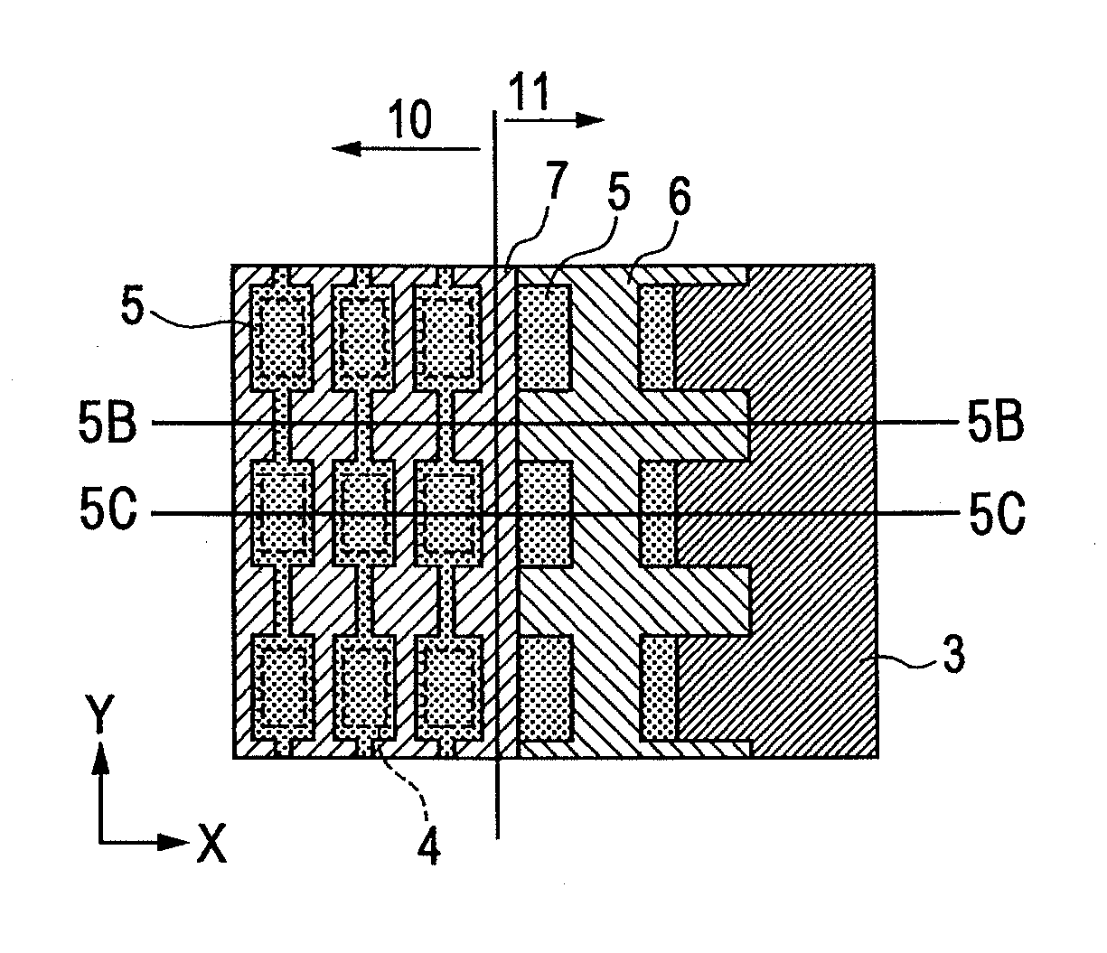
[0034]FIGS. 5A to 5C are partially enlarged plan views of the light emitting screen according to a second embodiment of the present invention and more specifically, illustrates a portion corresponding to the region 12 illustrated in FIG. 4. FIG. 5A is a partially enlarged plan view of the light emitting screen. FIG. 5B is a sectional view along line 5B-5B of FIG. 5A. FIG. 5C is a sectional view along line 5C-5C of FIG. 5A.

[0035]The present embodiment is the same as the first embodiment except that the face plate 1 as the light emitting screen has a different configuration of the peripheral region 11. In the first embodiment, the resistance layer 6 in the peripheral region 11 is uniformly formed (solid pattern), while in the present embodiment, the resistance layer 6 in the peripheral region 11 has a plurality of apertures formed in a lattice pattern (see FIG. 5A). The anodes 5 are formed on the resistance layer 6 and in the plurality of apertures. Each anode 5 in the peripheral regi...

third embodiment

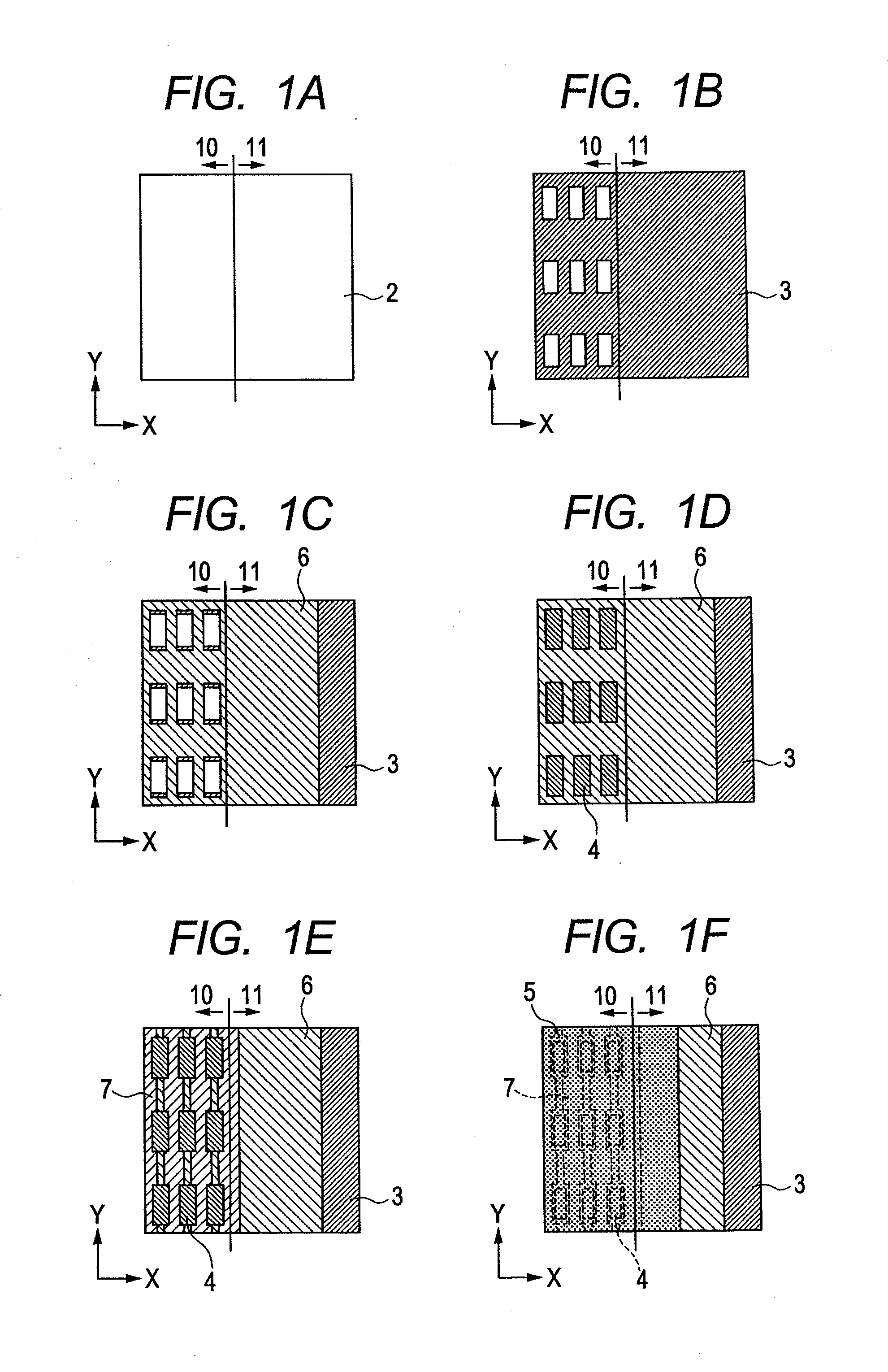
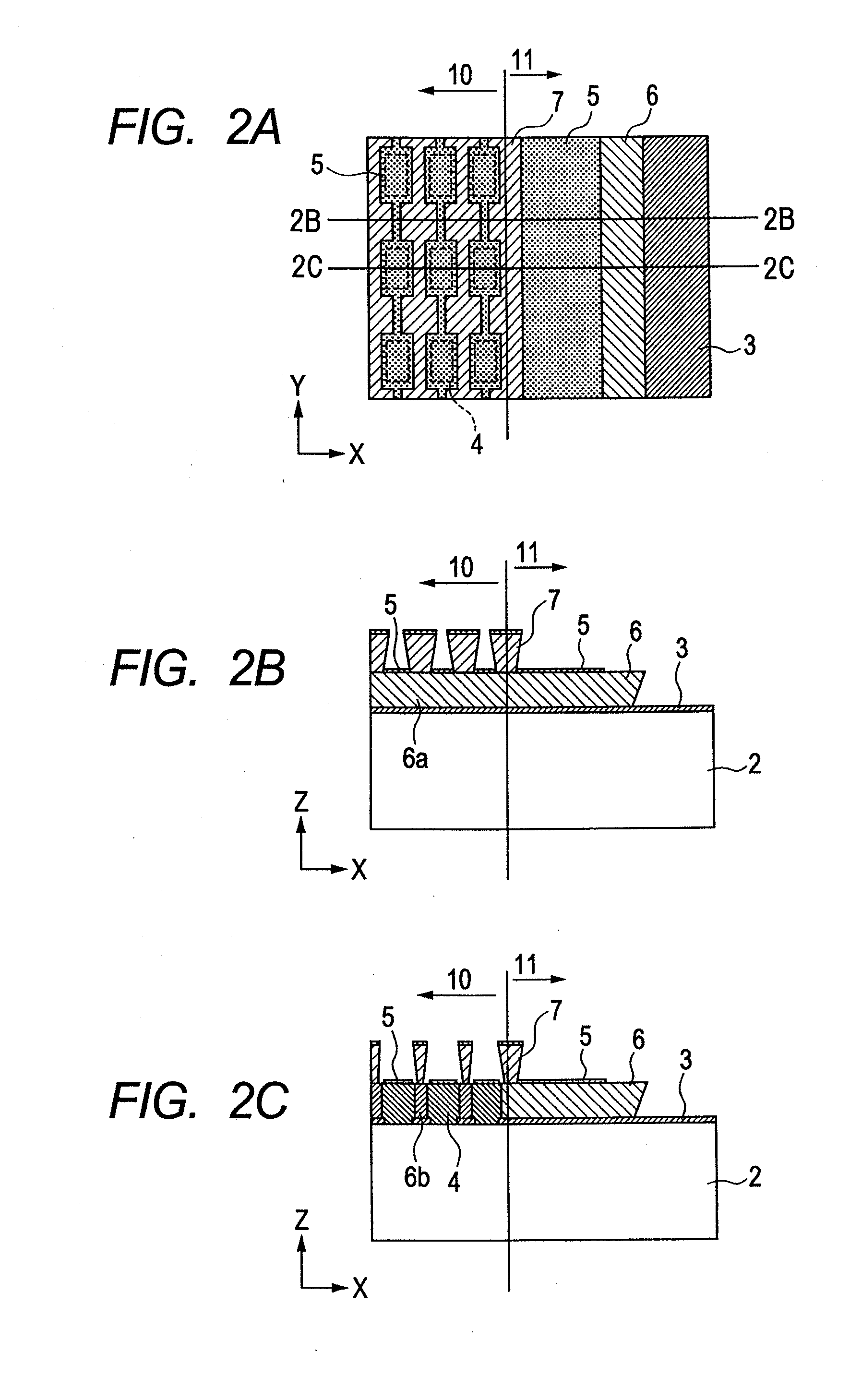
[0037]FIGS. 6A to 6C are partially enlarged plan views of the light emitting screen according to a third embodiment of the present invention and more specifically, illustrates a portion corresponding to the region 12 illustrated in FIG. 4. FIG. 6A is a plan view of the portion of the light emitting screen. FIG. 6B is a sectional view along line 6B-6B of FIG. 6A. FIG. 6C is a sectional view along line 6C-6C of FIG. 6A.

[0038]The present embodiment is the same as the first embodiment except that the resistance adjusting layer 7 is also formed in the peripheral region 11 outside the image display region 10.

[0039]The resistance adjusting layer 7 is formed so as to divide the peripheral region 11 into a plurality of regions. Each anode 5 is formed on the resistance layer 6 in a region divided by the resistance adjusting layer 7. The structure in which the anode 5 in the peripheral region 11 is divided into a plurality of portions may be the same as the divided region formed in the second ...


PUM


Abstract

A method of fabricating a light emitting screen 1 comprises steps of providing a resistance layer 6 having a plurality of apertures arranged in a lattice pattern and having light emitting members each arranged in each of the apertures, on a substrate 2 having an image display region 10 and a peripheral region 11 at an outer periphery of the image display region, such that the resistance layer extends from the image display region to the peripheral region, and such that the plurality of apertures are arranged in the image display region, providing a resistance adjusting layer having a resistance value larger than that of the resistance layer, on the resistance layer, to divide the image display region and the peripheral region into a plurality of segments, and forming a film of an electroconductive layer to cover the resistance layer and the light emitting member positioned in the segments.

Description

BACKGROUND OF THE INVENTION[0001]1. Field of the Invention[0002]The present invention relates to a light emitting screen for use in an image display apparatus and a method of fabricating the light emitting screen. In particular, the present invention relates to a light emitting screen having a light emitting member which displays an image by emitting light by irradiation of an electron beam emitted from an electron-emitting device, and a method of fabricating the light emitting screen.[0003]2. Description of the Related Art[0004]The image display apparatus using the electron-emitting device accelerates the electron beam by applying a voltage several-kV higher than that of the electron-emitting device to a phosphor surface. Unfortunately, the distance between the phosphor surface and the electron-emitting device is about 1 to 2 mm, and thus an intense electric field is formed. The intense electric field often causes discharge. In order to restrict current from flowing when a discharg...

Claims


Application Information

Patent Timeline
IPC IPC(8): H01J1/62H01J9/00
CPCH01J9/148H01J29/322H01J29/28
Inventor TOYOGUCHI, GINJIRO
Owner CANON KK
Why Eureka
Try Eureka