Photoelectric conversion device manufacturing method, photoelectric conversion device, photoelectric conversion device manufacturing system, and method for using photoelectric conversion device manufacturing system

Inactive Publication Date: 2012-01-19
ULVAC INC
View PDF0 Cites 6 Cited by
  • Summary
  • Abstract
  • Description
  • Claims
  • Application Information

AI Technical Summary

Benefits of technology

[0091]According to the photoelectric conversion device manufacturing method of the invention, the second i-type semiconductor layer is formed in the second plasma CVD reaction chamber, and the second plasma CVD reaction chamber is different from a plurality of the first plasma CVD reaction chambers in which the first p-type semiconductor layer, the first i-type semiconductor layer, the first n-type semiconductor layer, and the second p-type semiconductor layer are formed.
[0092]Because of this, impurities in the p-layer are not diffused in the second i-type semiconductor layer, or it is possible to prevent an indistinct junction which is caused by remaining impurities of the first plasma CVD reaction chamber being doped into a p-layer or an n-layer from being generated.
[0093]Additionally, since the second p-type semiconductor layer is exposed to an air atmosphere, an OH is adhered to the surface of the second p-type semiconductor layer, a part of the surfa

Problems solved by technology

However, in contrast, in the photoelectric conversion device in which the silicon single crystal is utilized, single crystal silicon ingot is sliced, a sliced silicon wafer is used in the solar cell; therefore, a large amount of energy is spent for manufacturing the ingot, and the manufacturing cost is high.
For example, at the moment, in a case of realizing a photoelectric conversion device having a large area which is placed outdoors or the like, when being manufactured by use of single crystal silicon, the cost considerably increases.
However, conversion efficiency of a photoelectric conversion device in which an amorphous-silicon thin film is utilized is lower than the conversion efficiency of a crystalline photoelectric conversion device in which single-crystalline silicon, polysilicon, or the like is utilized.
For this reason, there is a problem in that an indistinct junction which is caused by impurities in the p-layer being diffused in the i-layer or which is caused by remaining impurities in the reaction

Method used


Image

  • Photoelectric conversion device manufacturing method, photoelectric conversion device, photoelectric conversion device manufacturing system, and method for using photoelectric conversion device manufacturing system
  • Photoelectric conversion device manufacturing method, photoelectric conversion device, photoelectric conversion device manufacturing system, and method for using photoelectric conversion device manufacturing system
  • Photoelectric conversion device manufacturing method, photoelectric conversion device, photoelectric conversion device manufacturing system, and method for using photoelectric conversion device manufacturing system

Examples


first embodiment

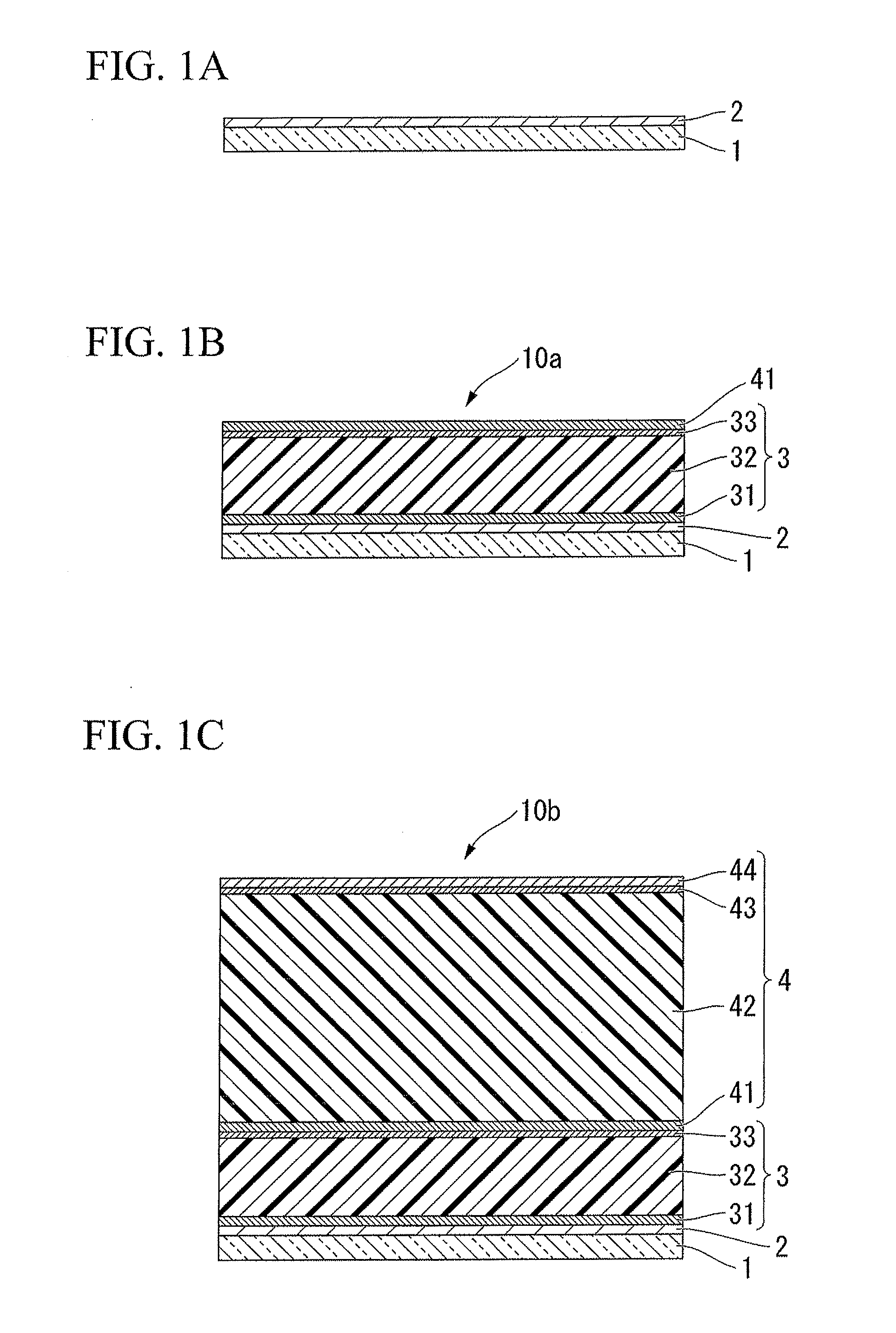
[0140]FIGS. 1A to 1C are cross-sectional views illustrating a photoelectric conversion device manufacturing method of the invention.

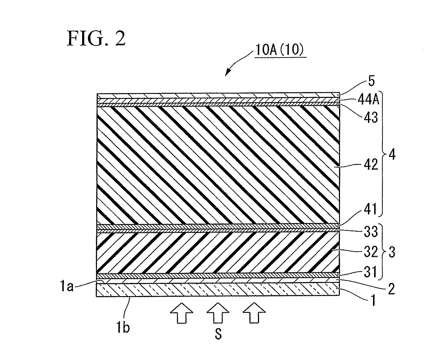
[0141]FIG. 2 is a cross-sectional view showing the layer structure of a photoelectric conversion device manufactured by the invention.

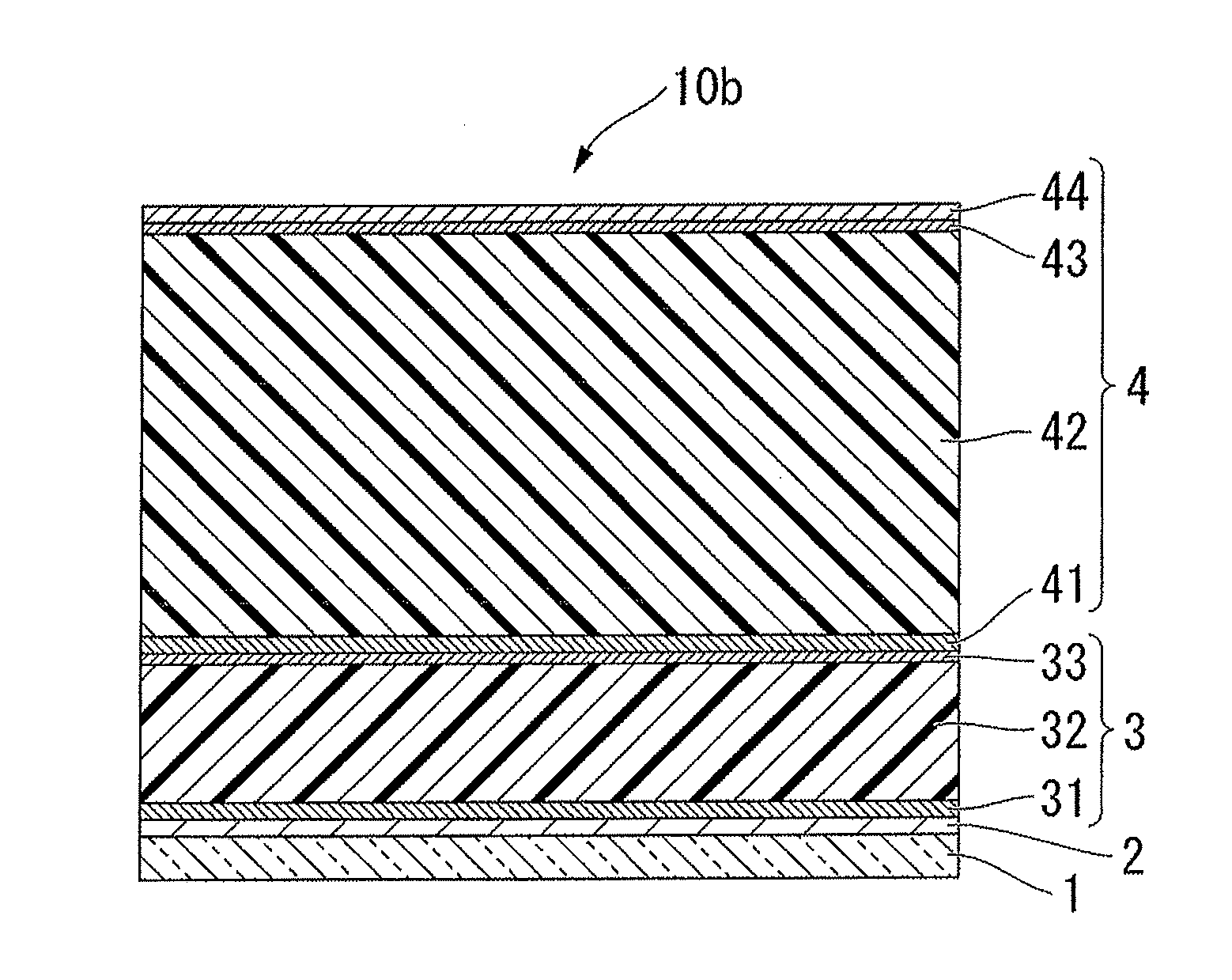
[0142]Firstly, as shown in FIG. 2, in the photoelectric conversion device 10A (10) manufactured by the manufacturing method of the invention, a first photoelectric conversion unit 3 and a second photoelectric conversion unit 4 are formed on a first face 1a (top face) of a substrate 1 in this order and stacked in layers.

[0143]Furthermore, a back-face electrode 5 is formed above the second photoelectric conversion unit 4.

[0144]Each of the first photoelectric conversion unit 3 and the second photoelectric conversion unit 4 includes a pin-type layer structure.

[0145]The substrate 1 is a substrate having optical transparency and insulation property and is composed of an insulation material having an excellent sunlight transpare...

second embodiment

[0311]Next, a second embodiment of the invention will be described.

[0312]In addition, in the explanation described below, identical symbols are used for the elements which are identical to those of the first embodiment, and the explanations thereof are omitted or simplified.

[0313]In the second embodiment, a constitution or a method which are different from the above-described first embodiment will be mainly described.

[0314]FIG. 4 is a cross-sectional view showing the layer structure of a photoelectric conversion device manufactured by a manufacturing method of a second embodiment.

[0315]In the second photoelectric conversion unit 4 of the photoelectric conversion device 10B (10), a p-type semiconductor layer 44B including oxygen (p-layer, third p-type semiconductor layer) is formed on the n-type semiconductor layer 43 (n-layer).

[0316]The p-layer 44B including oxygen is formed in the same reaction chamber as the reaction chamber in which the i-layer 42 and the n-layer 43 constituting ...

example 1

[0350]The photoelectric conversion device manufacturing method of Example 1 will be described.

[0351]A p-layer composed of an amorphous-silicon based thin film, a buffer layer, an i-layer composed of an amorphous-silicon based thin film, an n-layer including microcrystalline silicon, which constitute a first photoelectric conversion unit, and a p-layer including microcrystalline silicon and constituting the second photoelectric conversion unit were sequentially formed on a substrate.

[0352]In the method for forming the above layers, a plurality of plasma CVD reaction chambers which are connected in line were used, one layer was formed in one plasma CVD reaction chamber using a plasma CVD method, and a plurality of layers were formed by carrying out a step of transferring a substrate and a step of forming a film on the substrate in order.

[0353]Subsequently, the p-layer constituting the second photoelectric conversion unit was subjected to an air atmosphere, and an OH radical included p...


PUM

PropertyMeasurementUnit
Lengthaaaaaaaaaa
Electrical conductivityaaaaaaaaaa
Transparencyaaaaaaaaaa

Abstract

A photoelectric conversion device manufacturing method manufactures a photoelectric conversion device in which a first photoelectric conversion unit and a second photoelectric conversion unit are sequentially stacked on a transparent-electroconductive film formed on a substrate. The method includes: forming each of a first p-type semiconductor layer, a first i-type semiconductor layer, a first n-type semiconductor layer, and a second p-type semiconductor layer in a plurality of first plasma CVD reaction chambers; exposing the second p-type semiconductor layer to an air atmosphere; supplying a gas including p-type impurities to inside a second plasma CVD reaction chamber before forming of the second i-type semiconductor layer; forming the second i-type semiconductor layer on the second p-type semiconductor layer that was exposed to an air atmosphere, in the second plasma CVD reaction chamber; and forming the second n-type semiconductor layer on the second i-type semiconductor layer.

Description

BACKGROUND OF THE INVENTION[0001]1. Field of the Invention[0002]The present invention relates to a photoelectric conversion device manufacturing method, a photoelectric conversion device, a photoelectric conversion device manufacturing system, and a method for using a photoelectric conversion device manufacturing system.[0003]Specifically, the present invention relates to a technique in which a photoelectric conversion device having excellent efficiency can stably manufactured without degradation of characteristics and in which the cost and the efficiency of manufacturing can be improved, even in a case where the number of the processed substrates increases.[0004]This application claims priority from Japanese Patent Application No. 2009-020859 filed on Jan. 30, 2009, the contents of which are incorporated herein by reference in their entirety.[0005]2. Background Art[0006]In recent years, the photoelectric conversion devices have been widely used for solar cells, photodetectors, or t...

Claims


Application Information

Patent Timeline
IPC IPC(8): H01L31/0352H01L31/076
CPCC23C16/24C23C16/54H01L31/076H01L31/1804Y02E10/547H01L31/202Y02E10/545Y02E10/548H01L31/1824Y02P70/50C23C16/44H01L31/04H01L31/075H01L31/18
Inventor UCHIDA, HIROTOFUJINAGA, TETSUSHIWAKAI, MASAFUMIKOBAYASHI, TADAMASAUE, YOSHINOBUNAKAMURA, KYUZOASARI, SHINSAITO, KAZUYAMATSUMOTO, KOICHISHIMIZU, YASUOMORI, KATSUHIKO
Owner ULVAC INC
Why Eureka
Try Eureka