Optoelectronic devices with embedded void structures

a technology of optoelectronic devices and void structures, applied in semiconductor devices, lasers, semiconductor lasers, etc., can solve the problems of reducing the area available for overgrowth, making the fabrication of embedded gratings for optoelectronic devices much more difficult, and being more sensitive to inhomogeneity. , to achieve the effect of high diffraction efficiency and planar epitaxial growth

Inactive Publication Date: 2012-01-26
RGT UNIV OF CALIFORNIA
View PDF4 Cites 25 Cited by
  • Summary
  • Abstract
  • Description
  • Claims
  • Application Information

AI Technical Summary

Problems solved by technology

Therefore, a reduction on the periodicity of the grating results in a reduction on the area available for overgrowth, which makes the fabrication of embedded gratings for optoelectronic devices much more difficult and more sensitive to inhomogeneities in the dielectric stripes, as well as to the remaining dielectric material inside or close to the opening edges of the stripes.

Method used


Image

  • Optoelectronic devices with embedded void structures
  • Optoelectronic devices with embedded void structures
  • Optoelectronic devices with embedded void structures

Examples


Embodiment Construction

[0033]In the following description of the preferred embodiment, reference is made to the accompanying drawings which form a part hereof, and in which is shown by way of illustration a specific embodiment in which the invention may be practiced. It is to be understood that other embodiments may be utilized and structural changes may be made without departing from the scope of the present invention.

[0034]Overview

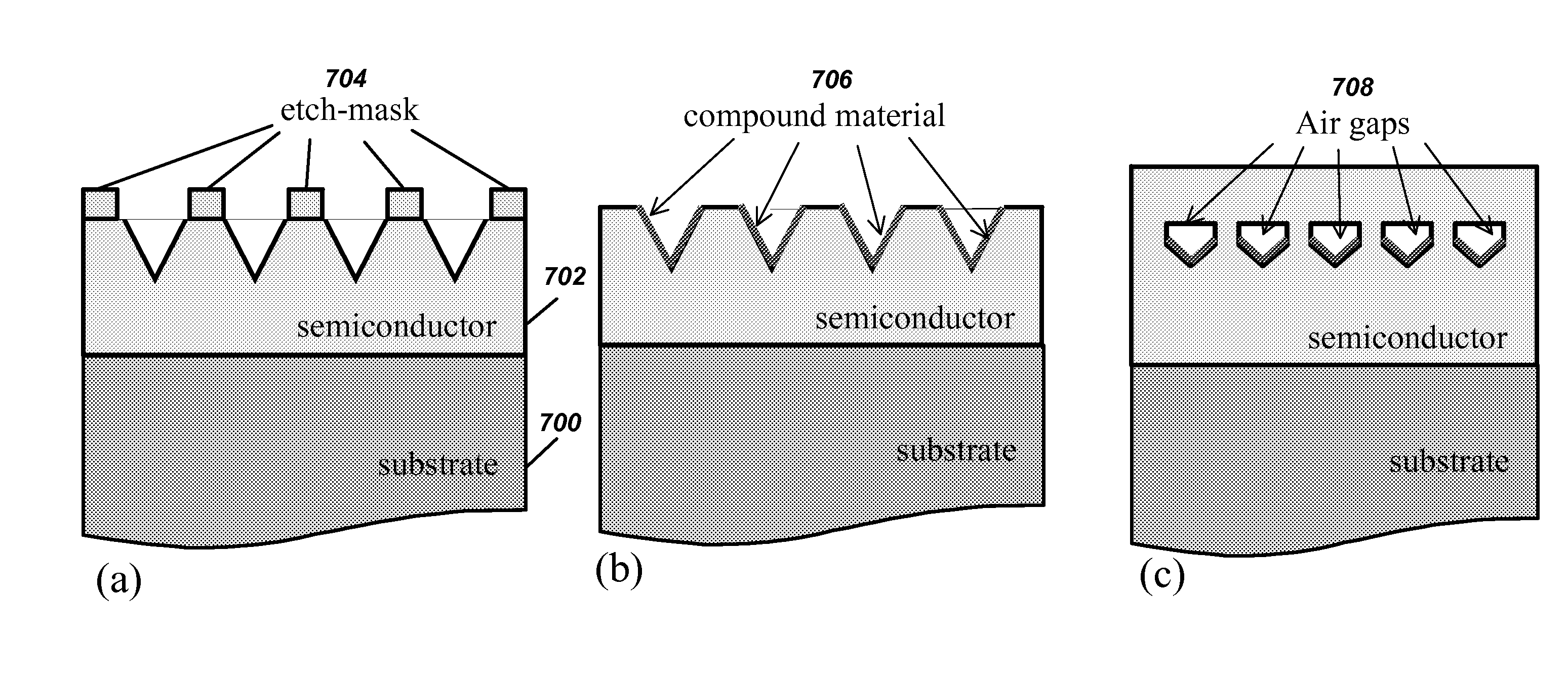
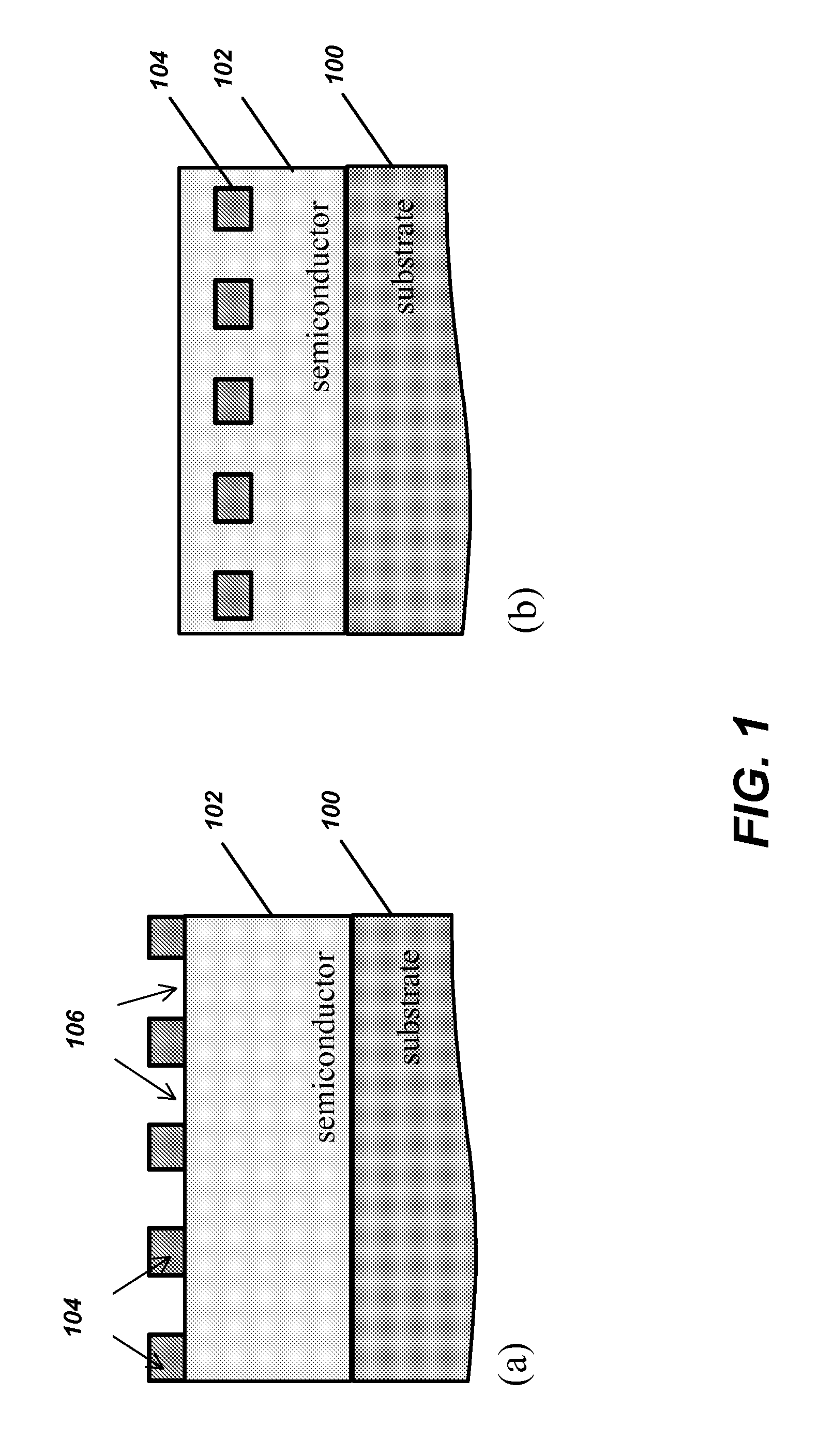
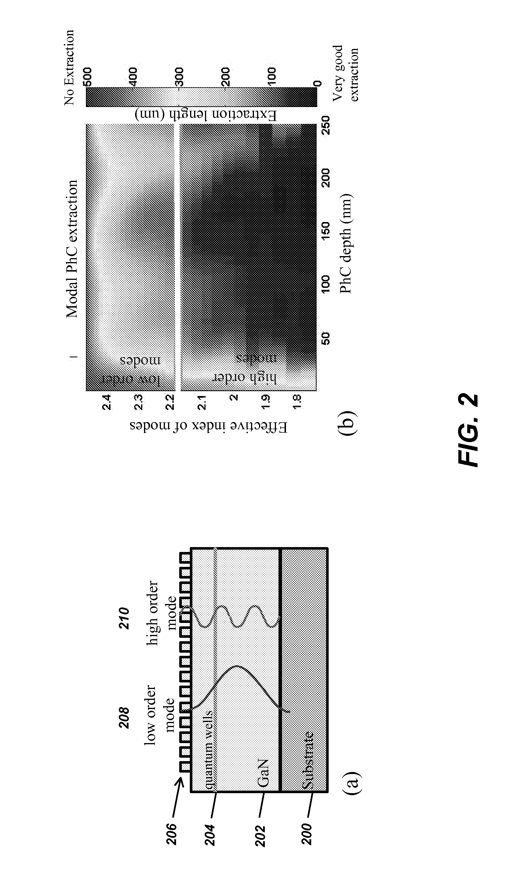
[0035]The present invention discloses a highly efficient optoelectronic structure based on growth of embedded PhCs on a semiconductor slab. The PhCs are gratings having void-gaps, air-gaps, or material voids, which results in a very high index contrast with other adjacent material layers and, consequently, a very high PhC diffraction strength. In one embodiment, a layer above the embedded void-gap PhCs is thin enough to provide a very high interaction between the electromagnetic guided modes in the semiconductor and the PhCs. Since the gaps within the PhCs are voids, the diffr...


PUM


Abstract

An optoelectronic structure, and method of fabricating same, comprised of semiconductors having growth-embedded void-gap gratings or photonic crystals in one or two dimensions, which are optimized to yield high interaction of the guided light and the photonic crystals and planar epitaxial growth. Such structure can be applied to increase light extraction efficiency in LEDs, increase modal confinement in lasers or increase light absorption in solar cells. The optimal dimensions of the growth-embedded void-gap gratings or photonic crystals are calculated by numerical simulation using scattering matrix formalism. The growth-embedded void-gap gratings are applicable to any semiconductor device, as well as optoelectronic devices, such as light-emitting diodes, laser diodes and solar cells.

Description

CROSS-REFERENCE TO RELATED APPLICATIONS[0001]This application claims priority under 35 U.S.C. §119(e) to co-pending and commonly-assigned U.S. Provisional Patent Application Ser. No. 61 / 367,239, filed on Jul. 23, 2010, by Elison de Nazareth Matioli, Claude C. A. Weisbuch, James S. Speck, and Evelyn L. Hu, and entitled “OPTOELECTRONIC DEVICES WITH EMBEDDED VOID STRUCTURES,” attorney's docket number 30794.385-US-P1 (2009-493-1), which application is incorporated by reference herein.[0002]This application is related to co-pending and commonly-assigned:[0003]U.S. Utility application Ser. No. 12 / 793,862, filed Jun. 4, 2010, by Claude C. A. Weisbuch, Aurelien J. F. David, James S. Speck, and Steven P. DenBaars, entitled “SINGLE OR MULTI-COLOR HIGH EFFICIENCY LIGHT EMITTING DIODE (LED) BY GROWTH OVER A PATTERNED SUBSTRATE,” attorneys' docket number 30794.122-US-C2 (2005-145-3), which application is a continuation of:[0004]U.S. Utility application Ser. No. 11 / 923,414, filed Oct. 24, 2007, b...

Claims


Application Information

Patent Timeline
Patent Type & Authority Applications(United States)
IPC IPC(8): H01L33/10H01L31/18H01L31/0232
CPCB82Y20/00H01L33/0079H01L33/22H01S5/34333H01L2933/0083H01S5/1017H01S5/105H01L33/508H01L33/0093H01S5/11
Inventor MATIOLI, ELISON DE NAZARETHWEISBUCH, CLAUDE C. A.SPECK, JAMES S.HU, EVELYN L.
Owner RGT UNIV OF CALIFORNIA
Why Eureka
Try Eureka