Chip scale package and fabrication method thereof

a technology of chip scale and scale plate, which is applied in the direction of semiconductor devices, semiconductor/solid-state device details, electrical apparatus, etc., can solve the problems of affecting the electrical connection between the electrode pads, the surface area of the mounting plate is not large enough, and the application of the rdl technique or disposing of conductive traces on the chip is limited, so as to avoid adhesive residue and avoid warpage of the package

Active Publication Date: 2012-01-26
SILICONWARE PRECISION IND CO LTD
View PDF6 Cites 26 Cited by
  • Summary
  • Abstract
  • Description
  • Claims
  • Application Information

AI Technical Summary

Benefits of technology

[0028]According to the present invention, a composite board comprising a hard layer and a soft layer is provided, wherein the soft layer has opposite first and second surfaces and the hard layer is disposed on the second surface of the soft layer, a chip is mounted on a carrier board first and then embedded in the first surface of the soft layer, and subsequently the carrier board is removed so as to allow a redistribution layer (RDL) process to be performed, thereby solving the conventional problems caused by directly attaching the chip on an adhesive film, such as film-softening caused by heat, encapsulant overflow, chip deviation and contamination and further preventing poor electrical connection between the wiring layer and the chip electrode pads in the subsequent RDL process and low product yield. Furthermore, through the use of the composite board, the present invention avoids warpage of the package and also eliminates the need of an additional hard carrier for fixing the package in a RDL process and accordingly avoids adhesive residue as in the prior art.

Problems solved by technology

However, the application of the RDL technique or disposing of conductive traces on the chip is limited by the size of the chip or the area of the active surface of the chip.
Particularly, as chips are developed towards high integration and compact size, they do not have enough surface area for mounting of more solder balls for electrical connection to an external device.
However, since the chip 12 is fixed by being attached to the adhesive film 11, deviation of the chip 12 can easily occur due to film-softening and extension caused by heat, especially in the package molding process, thereby adversely affecting the electrical connection between the electrode pads 120 of the chip 12 and the wring layer 15 during the subsequent RDL process.
Referring to FIG. 2, in another package molding process, since the adhesive film 11′ can easily be softened by heat, overflow 130 of the encapsulant 13 can easily occur to the active surface 121 of the chip 12 and even contaminate the electrode pads 120 of the chip 12, thus resulting in poor electrical connection between the electrode pads and subsequently formed wiring layer and even causing product failure.

Method used


Image

  • Chip scale package and fabrication method thereof
  • Chip scale package and fabrication method thereof
  • Chip scale package and fabrication method thereof

Examples


Embodiment Construction

[0037]The following illustrative embodiments are provided to illustrate the disclosure of the present invention, these and other advantages and effects can be apparent to those in the art after reading this specification.

[0038]It should be noted that the drawings are only for illustrative purposes and not intended to limit the present invention. Meanwhile, terms such as ‘first’, ‘second’, ‘up’, ‘down’, ‘inside’ etc. are only used as a matter of descriptive convenience and not intended to have any other significance or provide limitations for the present invention.

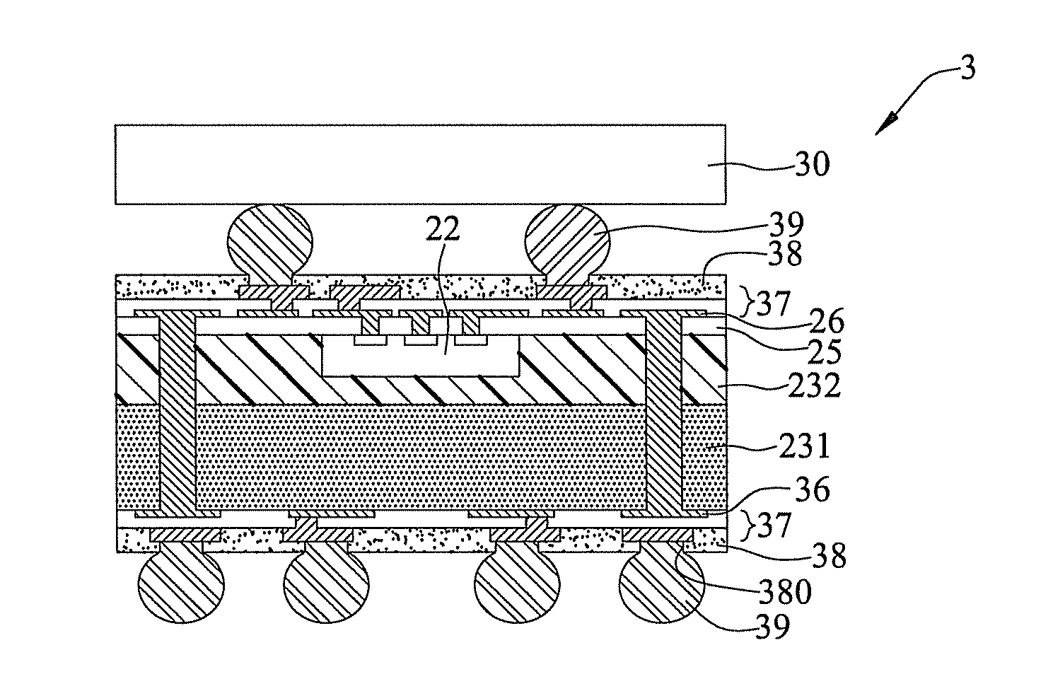
[0039]FIGS. 4A to 4H are cross-sectional views showing a fabrication method of a chip scale package according to the present invention.

[0040]Referring to FIG. 4A, a carrier board 20 having an adhesive layer 21 is provided. Referring to FIG. 4B, a chip 22 having an active surface 22a with a plurality of electrode pads 220 and an inactive surface 22b opposite to the active surface 22a is provided and disposed on the adhesive ...


PUM


Abstract

A fabrication method of a chip scale package includes: disposing a chip on a carrier board and embedding the chip into a composite board having a hard layer and a soft layer; and removing the carrier board so as to perform a redistribution layer (RDL) process, thereby solving the conventional problems caused by directly attaching the chip on an adhesive film, such as film-softening caused by heat, encapsulant overflow, chip deviation and contamination, etc., all of which may result in poor electrical connection between the wiring layer and the chip electrode pads in the subsequent RDL process and even waste products as a result.

Description

BACKGROUND OF THE INVENTION[0001]1. Field of the Invention[0002]The present invention relates generally to semiconductor packages and fabrication methods thereof, and more particularly, to a chip scale package and a fabrication method thereof.[0003]2. Description of Related Art[0004]A chip scale package (CSP) is characterized in that the package size is equivalent to the size of the chip that is disposed in the package. U.S. Pat. No. 5,892,179, No. 6,103,552, No. 6,287,893, No. 6,350,668 and No. 6,433,427 disclose a conventional CSP structure, wherein a built-up structure is directly formed on a chip without using a chip carrier, such as a substrate or a lead frame, and a redistribution layer (RDL) technique is used to accomplish a redistribution of the electrode pads of the chip to a desired pattern.[0005]However, the application of the RDL technique or disposing of conductive traces on the chip is limited by the size of the chip or the area of the active surface of the chip. Parti...

Claims


Application Information

Patent Timeline
Patent Type & Authority Applications(United States)
IPC IPC(8): H01L23/48H01L21/56H01L21/60
CPCH01L21/561H01L2224/16225H01L23/49827H01L23/5389H01L23/562H01L24/16H01L24/19H01L24/20H01L25/03H01L25/0655H01L2224/12105H01L2224/16227H01L2224/211H01L2224/221H01L2924/01029H01L2924/01082H01L2924/15311H01L2924/3511H01L2924/01006H01L2924/01033H01L2924/014H01L21/568H01L2224/05026H01L2224/05001H01L2224/05548H01L2924/00014H01L24/03H01L2924/0001H01L2224/02379H01L24/05H01L24/02H01L2224/05599H01L2224/05099H01L2224/02
Inventor CHANG, CHIANG-CHENGLIAO, HSIN-YICHANG, HSU-HISCHIU, SHIH-KUANG
Owner SILICONWARE PRECISION IND CO LTD
Why Eureka
Try Eureka