Writable Magnetic Memory Element

a magnetic memory element and magnetic field technology, applied in the field of magnetic elements, can solve the problems of increasing difficulty, affecting the operation of the device,

Active Publication Date: 2012-01-26
CENT NAT DE LA RECHERCHE SCI +4
View PDF4 Cites 51 Cited by
  • Summary
  • Abstract
  • Description
  • Claims
  • Application Information

AI Technical Summary

Benefits of technology

[0016]An object of the present invention is to provide a magnetic memory that, in order to invert magnetization, requires only the presence of a magnetic layer (having magnetization that is parallel or perpendicular to its plane) and that operates without the stack needing to pass a current perpendicularly to the planes of the layers.

Problems solved by technology

It is the very structure of a magnetic field, which by definition is not localized in three dimensions, that raises numerous difficulties for integrating magnetic fields in devices.
This problem becomes increasingly severe when the various memory or logic cells are located very close to one another in order to increase the density thereof.
At present, such incorporation encounters various difficulties that appear to be inter-related.
Nevertheless, tunnel junctions have the disadvantage of presenting large values for the product of resistance multiplied by area (RA).
Apart from the smallest value, the power dissipated in the junction is then large, which is harmful both in terms of energy consumption and in terms of damaging said junction.
To summarize, a difficulty lies in the impossibility of independently optimizing reading and writing since, in known STT devices, those two phenomena are intrinsically linked.
Another difficulty lies in the fact that writing requires current to be passed through the stack at very high density.
Yet another difficulty that is inherent to this link comes from the ever-greater complexity of the stacks.
This then gives rise to difficulties during structuring steps, and in particular during the etching step, which is one of the major blocking points for integrating such magnetic stacks.

Method used


Image

  • Writable Magnetic Memory Element
  • Writable Magnetic Memory Element
  • Writable Magnetic Memory Element

Examples


Embodiment Construction

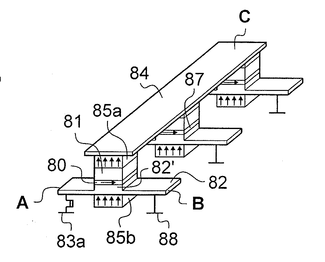
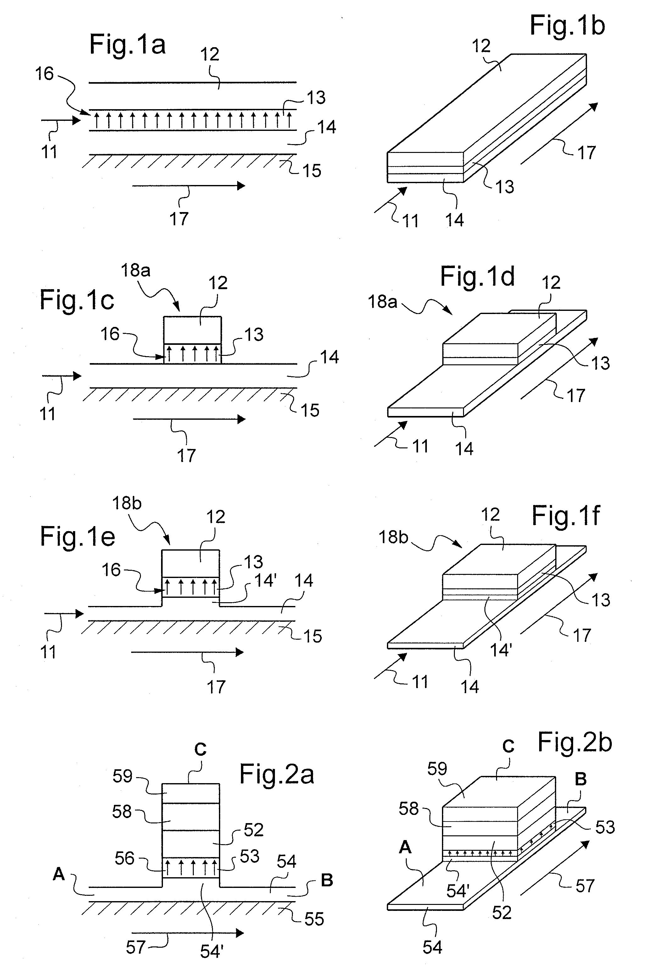
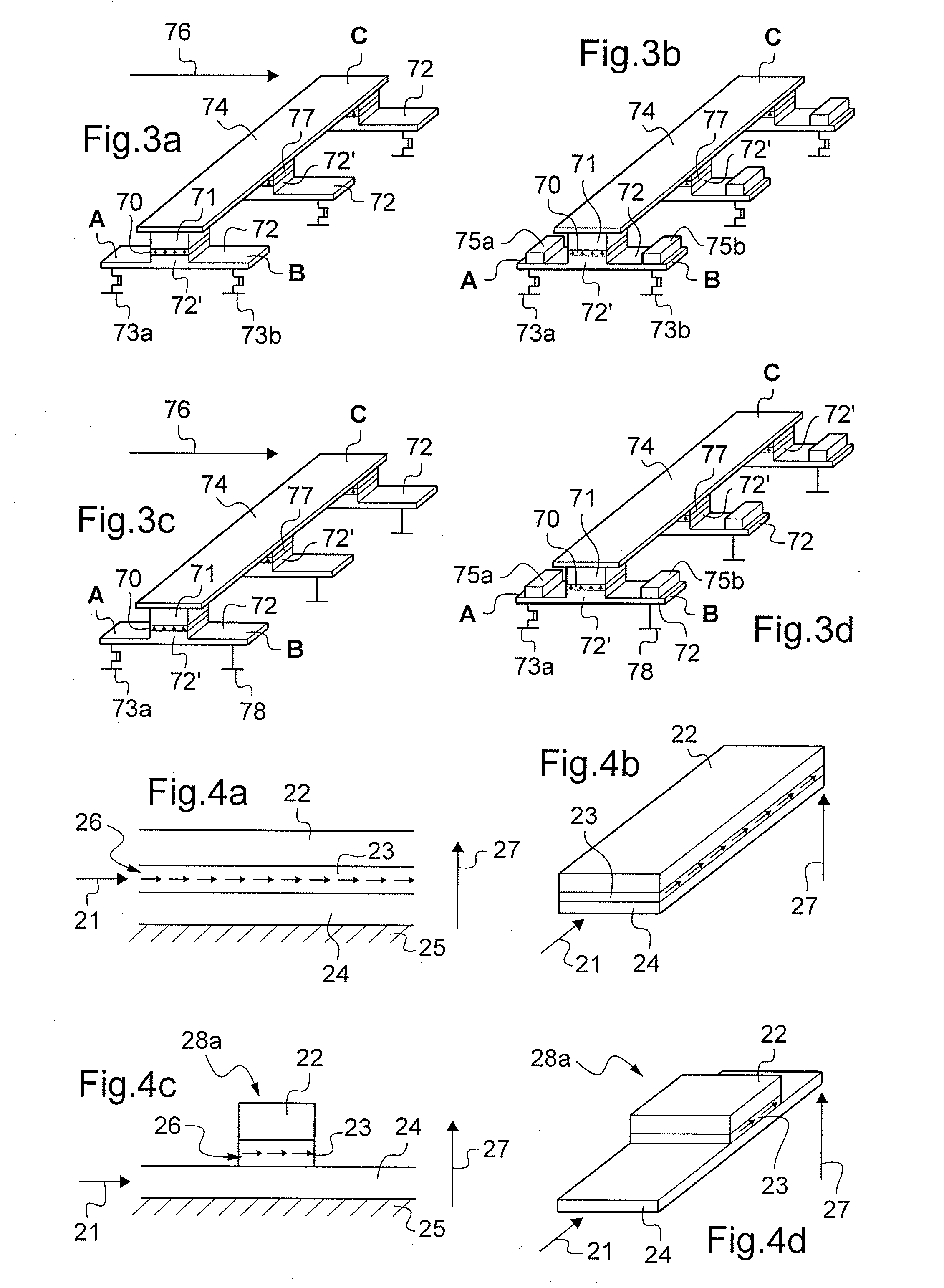
[0042]The stack implemented in the context of the present invention, i.e. a central magnetic layer sandwiched between two outer layers that are not magnetic, and at least one of which is conductive, the two outer layers being of different materials, has the effect of creating inversion asymmetry that generates a non-compensated electric field in the magnetic central layer. The electrons propagating in this electric field are subjected in their own frame of reference to a magnetic field known as the Rashba field {right arrow over (H)}R of direction that is perpendicular both to the current and to the electric field. This magnetic field is thus applied to the conduction electrons.

[0043]The inventors have shown that an effective magnetic field resulting from the Rashba field and the exchange interaction coupling the spin of the itinerant and localized electrons is applied on the local magnetization. Thus, the article by Joan Mihai Miron et al. entitled “Current-driven spin torque induc...


PUM


Abstract

The invention relates to a writable magnetic element comprising a stack of layers presenting a write magnetic layer, wherein the stack has a central layer of at least one magnetic material presenting a direction of magnetization that is parallel or perpendicular to the plane of the central layer, said central layer being sandwiched between first and second outer layers of non-magnetic materials, the first outer layer comprising a first non-magnetic material and the second outer layer comprising a second non-magnetic material that is different from the first non-magnetic material, at least the second non-magnetic material being electrically conductive, wherein it includes a device for causing current to flow through the second outer layer and the central layer in a current flow direction parallel to the plane of the central layer, and a device for applying a magnetic field having a component along a magnetic field direction that is either parallel or perpendicular to the plane of the central layer and the current flow direction, and wherein the magnetization direction and the magnetic field direction are mutually perpendicular.

Description

FIELD OF THE INVENTION[0001]The present invention provides a writable magnetic element of the current-induced reversal type.BACKGROUND OF THE INVENTION[0002]The magnetization of a layer or of a small magnetic element is commonly reversed by means of an applied magnetic field. The direction of the field is changed depending on whether it is desired to turn the magnetization in one direction or in another. Writing on magnetic tracks or on computer hard disks is based on this principle: the element for reversing is placed mechanically in the vicinity of a magnetic field generator so as to localize the field in three dimensions. It is the very structure of a magnetic field, which by definition is not localized in three dimensions, that raises numerous difficulties for integrating magnetic fields in devices. Thus, when no mechanical action is possible or desired, e.g. with solid magnetic memories known as magnetic random access memories (MRAM) or with logic devices, it is necessary to fo...

Claims


Application Information

Patent Timeline
Patent Type & Authority Applications(United States)
IPC IPC(8): G11C11/14H01L29/82
CPCG11C11/16G11C11/1675G11C11/161G11C11/1659G11C11/1673G11C11/18
Inventor GAUDIN, GILLESMIRON, IOAN MIHAIGAMBARDELLA, PIETROSCHUHL, ALAIN
Owner CENT NAT DE LA RECHERCHE SCI
Why Eureka
Try Eureka