Nb-DOPED PEROVSKITE FLUX PINNING OF REBCO BASED SUPERCONDUCTORS BY MOCVD

a technology of rebco and perovskite, applied in the direction of thin material processing, coating, electrical equipment, etc., can solve the problems of superconductor film reducing, critical current density, and first hts tape suffering from unacceptably low critical current densities

Inactive Publication Date: 2012-02-09
UT BATTELLE LLC
View PDF5 Cites 11 Cited by
  • Summary
  • Abstract
  • Description
  • Claims
  • Application Information

AI Technical Summary

Problems solved by technology

The first HTS tapes suffered from unacceptably low critical current densities, a problem caused by poor alignment of grains in the HTS film or coating.
A problem with HTS tapes and wires is that the critical current density (typically expressed as Jc) of the superconductor film decreases when the superconductor film is exposed to an external magnetic field.
The pinning defects have been found to significantly reduce current density losses in superconductor films in the presence of an external magnetic field.
Degradation of a high-temperature superconductor's properties due to flux creep is a limiting factor in the use of these superconductors.
However, the common techniques currently capable of producing such phase-separated substrates are not commercially viable.
For example, physical vapor deposition (PVD), pulsed laser deposition (PLD), molecular beam epitaxy (MBE), and atomic layer deposition (ALD) possess the significant drawbacks of being non-scalable, cost prohibitive, and industrially inefficient (i.e., the possibility of low throughput and higher cost).
Also, Zr doping can result in reduced superconducting transition temperature (Tc) and Jc performance, and has offered only limited pinning improvement for fields applied near the a-b axis of the REBCO film at 5-77 K.

Method used


Image

  • Nb-DOPED PEROVSKITE FLUX PINNING OF REBCO BASED SUPERCONDUCTORS BY MOCVD
  • Nb-DOPED PEROVSKITE FLUX PINNING OF REBCO BASED SUPERCONDUCTORS BY MOCVD
  • Nb-DOPED PEROVSKITE FLUX PINNING OF REBCO BASED SUPERCONDUCTORS BY MOCVD

Examples


Embodiment Construction

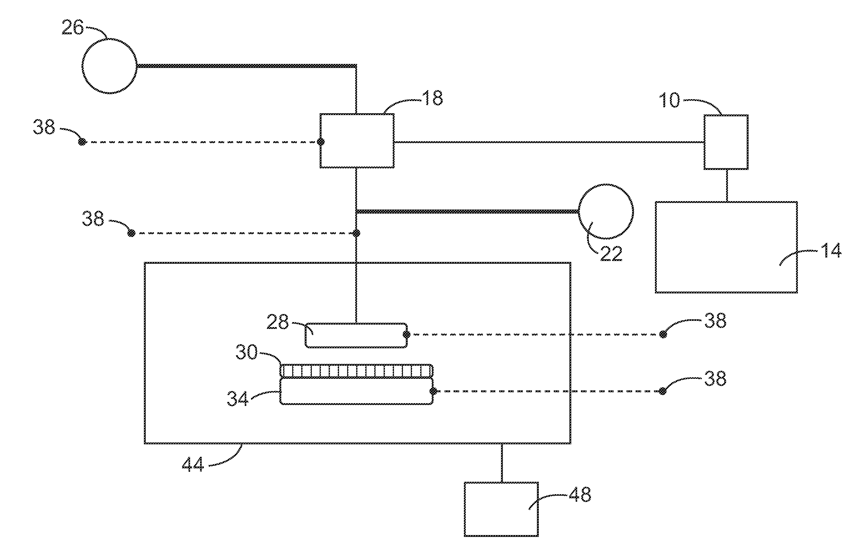
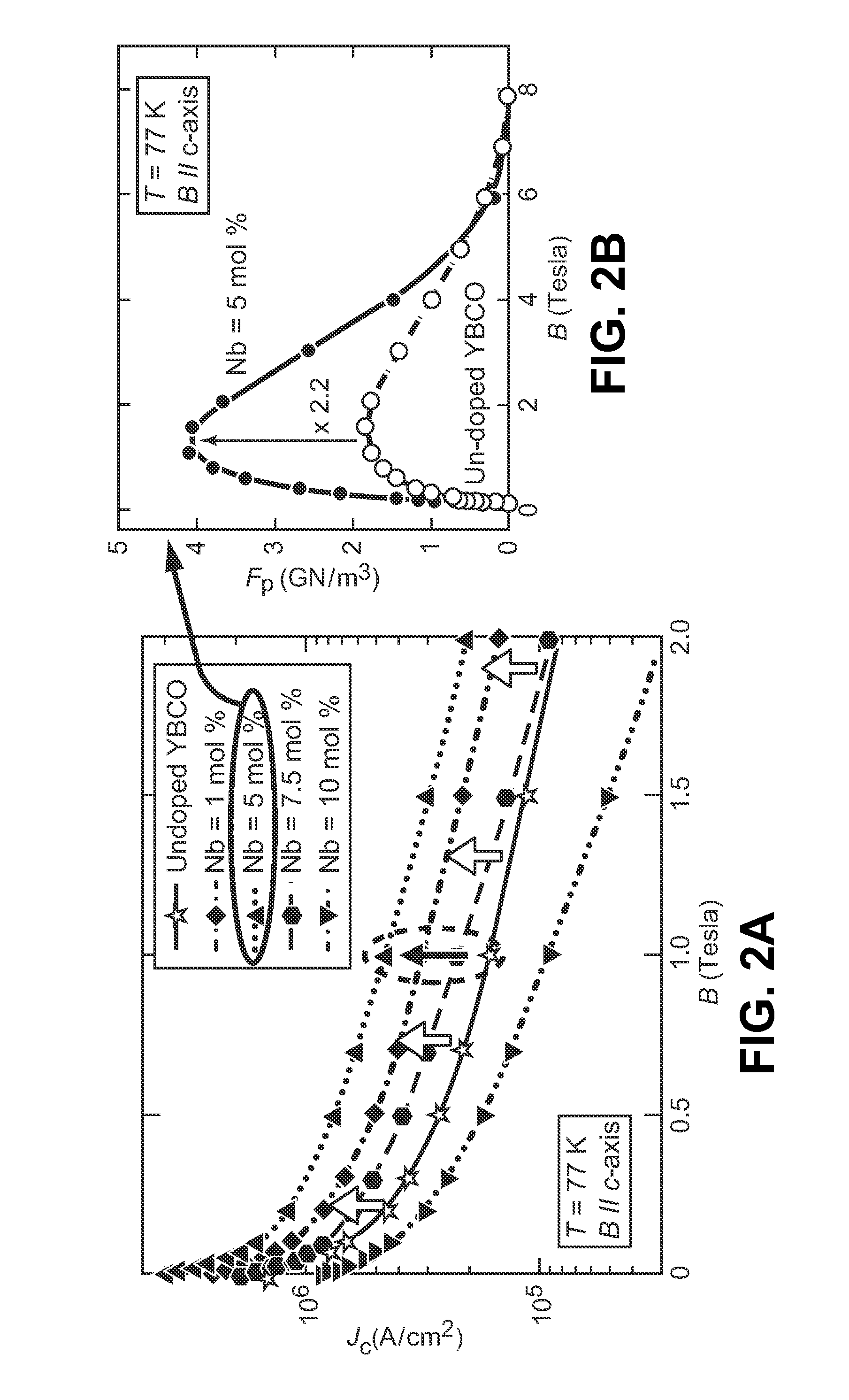
[0031]The present invention provides for the creation of pinning defects in superconducting films through the introduction of niobium (Nb), Tantalum (Ta) and / or Vanadium (V) compounds into the superconductor film during a MOCVD process. The defects are incorporated into the superconductor film as a secondary phase. This phase can be constituted by a perovskite or double perovskite or perovskite-like structure including the dopant. In the case of Nb, the secondary phase can comprise one or both of YpBaqNbrOs, where p=1±0.5, q=2±0.5, r=1±0.5, and s=6±0.5, such as YBa2NbO6, and BaxNbyOz, where x=0-14.66, y=1-17, and z=3-32. In the case of Ta, the secondary phase can comprise one or both of YBa2TaO6 and BaxTayOz, where x=0-7, y=1-6, z=1-16, and YxTayOz where x=1-10, y=1-7, z=3-25, and Ba(Y0.5Ta0.5)O3. In the case of V, the secondary phase can comprise one or some combination of YBa2VO6, YBa2V3O11, and BaxVyOz, where x=0-8, y=1-12, z=0.2-30, and YxVyOz where x=1-10, y=1-2, and z=4-20. Co...


PUM

PropertyMeasurementUnit
deposition pressureaaaaaaaaaa
deposition temperatureaaaaaaaaaa

Abstract

A method of making a superconducting article that involves using MOCVD to deposit onto a uniaxially or biaxially textured surface an epitaxial layer that includes a superconducting material such as REBa2Cu3O7 and a secondary phase comprising at least one dopant, the dopant including Nb, Ta and/or V, or combinations thereof.

Description

STATEMENT REGARDING FEDERALLY SPONSORED RESEARCH[0001]The United States Government has rights in this invention pursuant to contract no. DE-AC05-000R22725 between the United States Department of Energy and UT-Battelle, LLC.FIELD OF THE INVENTION[0002]The invention is drawn to flux pinning of REBCO based semiconductors using MOCVD techniques.BACKGROUND OF THE INVENTION[0003]Methods for the preparation of films of high temperature superconductor (HTS) materials on various substrates are well known. The first HTS tapes suffered from unacceptably low critical current densities, a problem caused by poor alignment of grains in the HTS film or coating. Several techniques have subsequently been developed to fabricate wires or tapes wherein grain alignment is produced, such as Rolling-Assisted-Biaxially-Textured-Substrates (RABiTS). RABiTS substrates typically include a textured metal underlayer (for example, nickel or nickel alloy) and an epitaxial buffer layer (for example, Y2O3 and / or ytt...

Claims


Application Information

Patent Timeline
Patent Type & Authority Applications(United States)
IPC IPC(8): H01L39/00H01L39/24
CPCH01L39/2441H01L39/2454Y10T428/24612H10N60/0464H10N60/0828H10N60/0576
Inventor AYTUG, TOLGAPARANTHAMAN, MARIAPPAN PARANSMARONI, VICTOR A.MILLER, DEAN J.
Owner UT BATTELLE LLC
Why Eureka
Try Eureka