Semiconductor device

a semiconductor and gate technology, applied in the direction of semiconductor devices, basic electric elements, electrical appliances, etc., can solve the problems of restricted hole injection from the igbt cell to the diode cell, reduced and reduced so as to reduce the resistance of the drift layer and reduce the steady loss of the igbt cell. , the effect of conducting modulation

Active Publication Date: 2012-02-23
DENSO CORP +1
View PDF2 Cites 84 Cited by
  • Summary
  • Abstract
  • Description
  • Claims
  • Application Information

AI Technical Summary

Benefits of technology

[0021]IGBT cell serves as the potential wall, the flow of holes from the drift layer to the channel layer is restricted when the IGBT cell is operated. Therefore, it is less likely that the holes will be discharged to the emi

Problems solved by technology

As a result, the resistance of the drift layer reduces, and thus steady loss of the IGBT cell

Method used


Image

  • Semiconductor device
  • Semiconductor device
  • Semiconductor device

Examples


first embodiment

[0055]A first embodiment of the present invention will be hereinafter described with reference to FIGS. 1 and 2. An insulated gate semiconductor device according to the present embodiment is, for example, used as a power switching device of a power supply circuit, such as an inverter and a DC / DC converter.

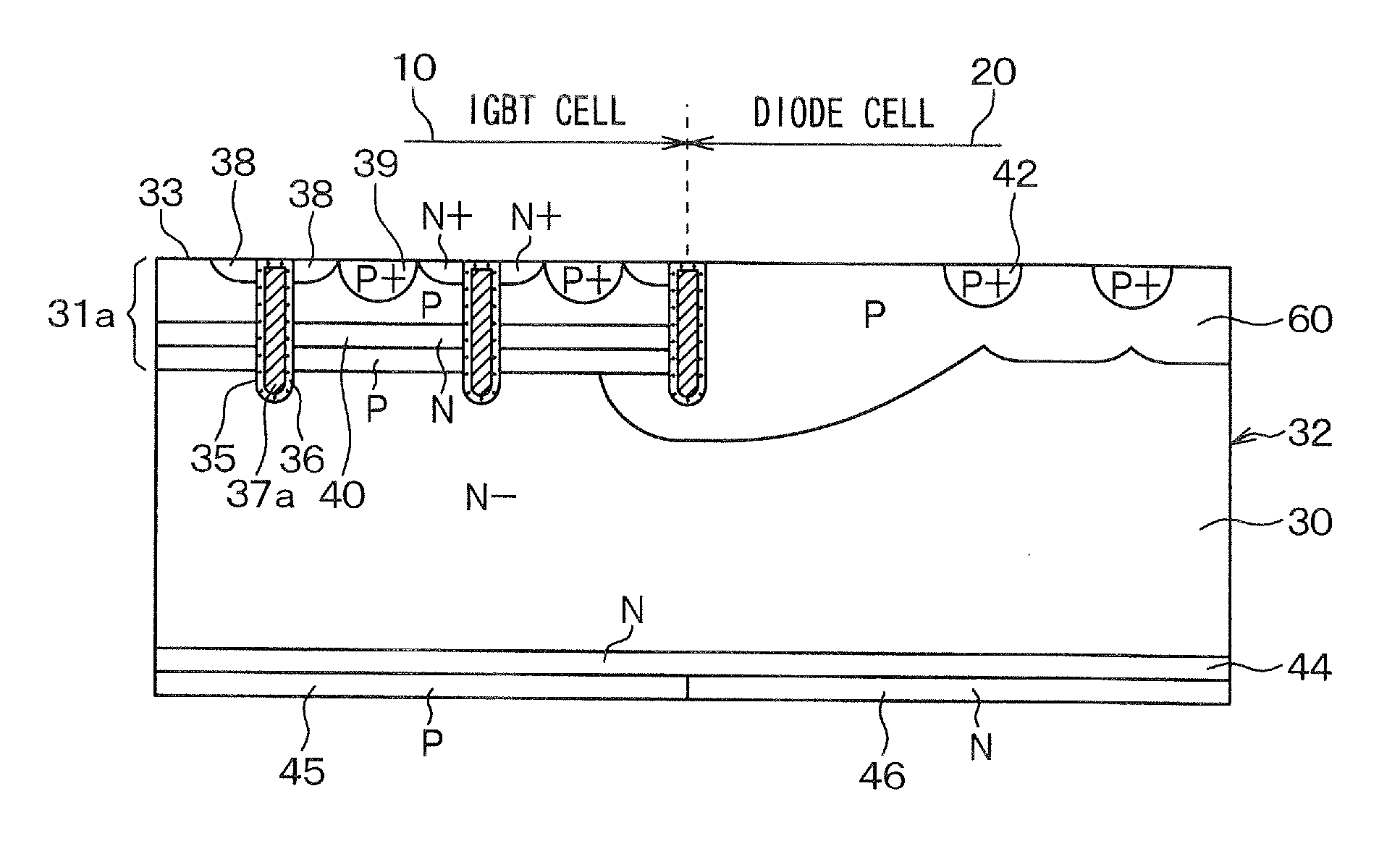
[0056]FIG. 1 is a cross-sectional view of a part of the semiconductor device according to the present embodiment. Referring to FIG. 1, the semiconductor device is a reverse conducting-insulated gate bipolar transistor (RC-IGBT) having an IGBT cell 10 and a diode cell 20 adjacent to the IGBT cell 10. The IGBT cell 10 forms a section in which multiple IGBT elements are formed, and the diode cell 20 forms a section in which a diode element is formed. Although not illustrated, multiple IGBT cells 10 and diode cells 20 are alternately disposed.

[0057]The IGBT cell 10 and the diode cell 20 commonly have a semiconductor substrate 32. The semiconductor substrate 32 has an N−-type drift laye...

second embodiment

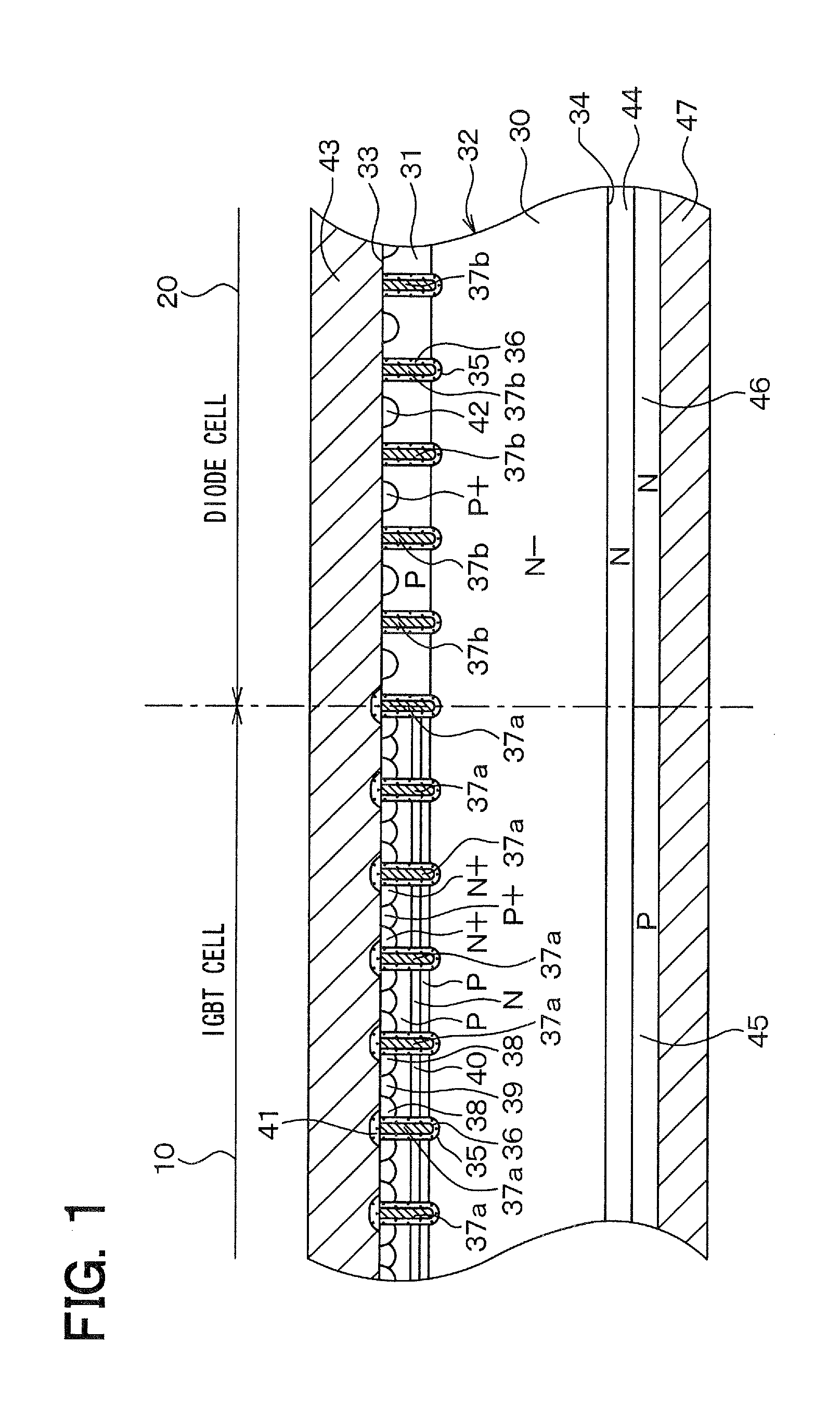
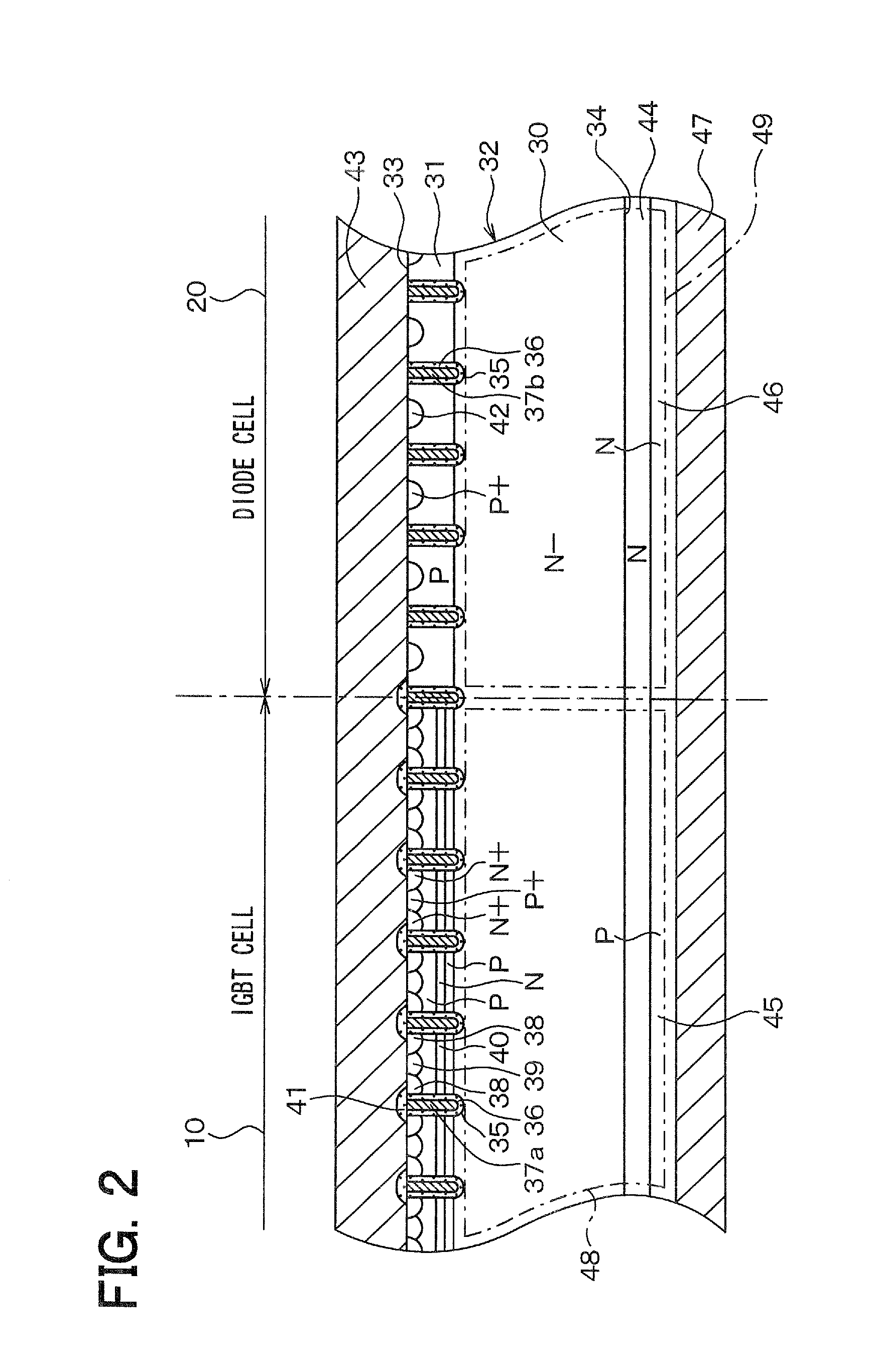
[0087]A second embodiment will be described with reference to FIGS. 3 through 5. Hereinafter, a structure different from the structure of the first embodiment will be mainly described.

[0088]FIG. 3 is a cross-sectional view of a semiconductor device according to the present embodiment. FIG. 4 is a plan view of an outer portion of the semiconductor device according to the present embodiment. FIG. 5 is a cross-sectional view taken along a line Va-Vb-Vc in FIG. 4. In FIG. 5, the collector electrode 47 is not illustrated for the purpose of simplicity.

[0089]Referring to FIG. 3, the interlayer insulating film 41 is formed on the base layer 31 of the diode cell 20, in addition to the base layer 31 of the IGBT cell 10. The interlayer insulating film 41 covers ends (e.g., upper ends in FIG. 3) of the trench electrodes 37b. In the diode cell 20, therefore, the trench electrodes 37b and the emitter electrode 43 are electrically insulated from each other by the interlayer insulating film 41. For...

third embodiment

[0098]A third embodiment will be described with reference to FIG. 6. Hereinafter, a structure different from the structure of the second embodiment will be mainly described.

[0099]In the second embodiment, the trench electrodes 37b are electrically connected to the emitter electrodes 43 at the longitudinal ends of the trenches 35 through the emitter leading electrode 50. In the present embodiment, the trench electrodes 37b are connected to a control electrode 56, which is different from the emitter electrode 43, at the longitudinal ends of the trenches 35.

[0100]FIG. 6 is a plan view of a part of a semiconductor device according to the present embodiment. As shown in FIG. 6, the emitter leading electrode 50 and the gate leading electrode 53 are disposed in the similar layout to those of the second embodiment. Further, the control electrode 56 is disposed between the emitter electrode 43 and the gate metal electrode 54.

[0101]The control electrode 56 is separated from the emitter electr...


PUM


Abstract

In a semiconductor device, an IGBT cell includes a trench passing through a base layer of a semiconductor substrate to a drift layer of the semiconductor substrate, a gate insulating film on an inner surface of the trench, a gate electrode on the gate insulating film, a first conductivity-type emitter region in a surface portion of the base layer, and a second conductivity-type first contact region in the surface portion of the base layer. The IGBT cell further includes a first conductivity-type floating layer disposed within the base layer to separate the base layer into a first portion including the emitter region and the first contact region and a second portion adjacent to the drift layer, and an interlayer insulating film disposed to cover an end of the gate electrode. A diode cell includes a second conductivity-type second contact region in the surface portion of the base layer.

Description

CROSS REFERENCE TO RELATED APPLICATION[0001]This application is based on Japanese Patent Applications No. 2010-182356 filed on Aug. 17, 2010 and No. 2010-195837 filed on Sep. 1, 2010, the disclosure of which are incorporated herein by reference.FIELD OF THE INVENTION[0002]The present invention relates to an insulated gate semiconductor device.BACKGROUND OF THE INVENTION[0003]A semiconductor device having an insulated gate bipolar transistor (IGBT) cell and a free wheeling diode (FWD) cell in the same semiconductor substrate has been proposed, for example, in JP 2007-214541A corresponding to U.S. 2007 / 0170549.[0004]In the semiconductor device, for example, a P-type layer is formed in a surface portion of an N-type semiconductor substrate, and an N-type emitter region is formed in a surface portion of the P-type layer. Further, first trenches are formed to reach the N-type semiconductor substrate while passing through the N-type emitter region and the P-type layer. A gate electrode is...

Claims


Application Information

Patent Timeline
IPC IPC(8): H01L29/739
CPCH01L29/0696H01L29/1095H01L29/407H01L29/7397H01L29/8613
Inventor KOYAMA, MASAKIOOKURA, YASUSHISOENO, AKITAKANAGAOKA, TATSUJISUGIYAMA, TAKAHIDEAOI, SACHIKOIGUCHI, HIROKO
Owner DENSO CORP
Why Eureka
Try Eureka