A kind of sic IGBT with low on-resistance and preparation method thereof

A low on-resistance, hole-blocking layer technology, applied in semiconductor/solid-state device manufacturing, circuits, electrical components, etc., to achieve the effects of enhanced conductance modulation, good turn-off loss, and good forward voltage drop

Active Publication Date: 2018-03-27
XIDIAN UNIV
View PDF6 Cites 0 Cited by
  • Summary
  • Abstract
  • Description
  • Claims
  • Application Information

AI Technical Summary

Problems solved by technology

[0004] For the traditional SiC IGBT structure, although its performance has been greatly improved compared with MOS and BJT, for high-voltage and high-power semiconductor devices, as the requirements for withstand voltage become higher and higher, the drift layer As the thickness continues to increase, the trade-off between on-resistance and switching loss has always been a problem in IGBT devices

Method used


Image

  • A kind of sic IGBT with low on-resistance and preparation method thereof
  • A kind of sic IGBT with low on-resistance and preparation method thereof

Examples


preparation example Construction

[0035] The embodiment of the present invention also provides a method for preparing the above-mentioned SiC IGBT, the method comprising the following steps:

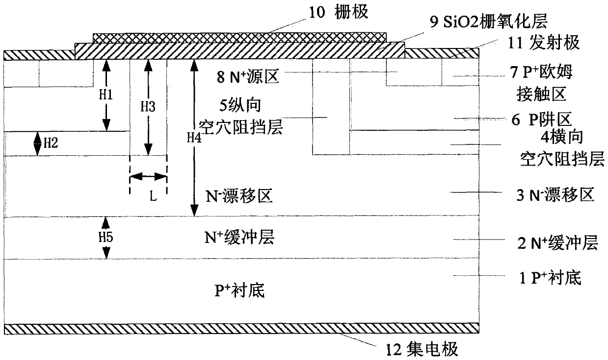
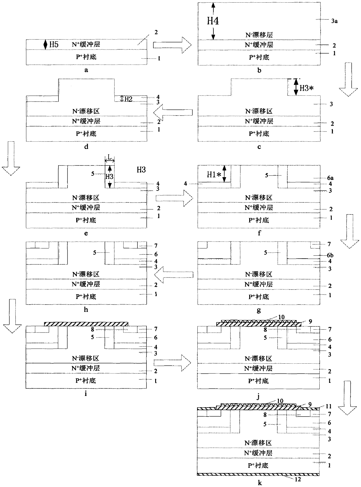
[0036] S1, such as figure 2 As shown in the figure a, N + buffer layer (2), the doping concentration of the N+ buffer layer (2) is 8×10 16 -3×10 17 cm -3 , the thickness H5 is 2-14 μm.

[0037] By chemical vapor deposition, the P + Epitaxial growth on the substrate (1) forms N + For the buffer layer (2), the epitaxial growth temperature is 1600° C., the pressure is 100 mbar, the reaction gas is silane and propane, the carrier gas is hydrogen, and the impurity source is liquid nitrogen.

[0038] S2, such as figure 2 b as shown in the N + Formation of N on the buffer layer (2) - drift layer (3a), the N - The doping concentration of the drift layer (3a) is 2×10 14 cm -3 , the thickness H4 is 100-180 μm.

[0039] Using chemical vapor deposition method, in N + epitaxial growth on the buffer layer (2) to form N...

Embodiment 1

[0051] Step 1 at P + Epitaxial growth of N on the substrate + buffer layer, such as figure 2 a.

[0052] Using RCA cleaning standards for P + The SiC substrate sample was cleaned, and the epitaxial growth thickness on the entire substrate surface was 2 μm, and the nitrogen ion doping concentration was 8×10 16 cm -3 N + buffer layer, such as figure 2 a. The process conditions are as follows: the epitaxial growth temperature is 1650°C, the pressure is 100mbar, the reaction gas is silane and propane, the carrier gas is hydrogen, and the impurity source is liquid nitrogen.

[0053] Step 2 at N + Epitaxial growth of N on the buffer layer - drift layer, such as figure 2 b.

[0054] in N + Epitaxial growth of N on the buffer layer - Drift layer, nitrogen ion doping concentration is 2×10 14 cm -3 , with a thickness of 100 μm, such as figure 2 b. The epitaxy process conditions are as follows: the epitaxial growth temperature is 1650°C, the pressure is 100mbar, the re...

Embodiment 2

[0090] Step A in P + Epitaxial growth of N on SiC substrate samples + buffer layer, such as figure 2 a.

[0091] Using RCA cleaning standards for P + The SiC substrate sample was cleaned, and the epitaxial growth thickness on the entire substrate surface was 8 μm, and the nitrogen ion doping concentration was 1×10 17 cm -3 N + buffer layer, such as figure 2 a. The process conditions are as follows: the epitaxial growth temperature is 1650°C, the pressure is 100mbar, the reaction gas is silane and propane, the carrier gas is hydrogen, and the impurity source is liquid nitrogen.

[0092] Step B at N + Epitaxial growth of N on the buffer layer - drift layer, such as figure 2 b.

[0093] in N + Epitaxial growth of N on the buffer layer - Drift layer, nitrogen ion doping concentration is 2×10 14 cm -3 , with a thickness of 140 μm, such as figure 2 b. The epitaxy process conditions are as follows: the epitaxial growth temperature is 1650°C, the pressure is 100mbar...


PUM


Abstract

The embodiment of the invention provides a low-on-resistance SiC IGBT and a manufacturing method of the SiC IGBT, and relates to the technical field of high-voltage power semiconductor devices. The conductivity of a drift region can be improved, the connecting voltage drop and on resistance of the devices can be reduced, and therefore forward connecting power consumption is reduced. A SiC IGBT comprises a P+ substrate (1), an N+ buffer layer (2), an N- drift region (3), an N+ hole blocking layer (4), an N+ hole blocking layer (5), a P well region (6), a P+ Ohmic contact region (7), an N+ source region (8), a SiO2 gate oxide layer (9), a grid electrode (10), an emitting electrode (11) and a collector electrode (12), the transverse N+ hole blocking layer (4) and the longitudinal N+ hole blocking layer (5) are arranged between the P well region (6) and the N- drift region (3), and the P well region (6), the N+ hole blocking layer (4) and the N+ hole blocking layer (5) are all constantly doped.

Description

technical field [0001] The invention relates to the technical field of high-voltage power semiconductor devices, in particular to a low on-resistance SiC (silicon carbide) IGBT (Insulated Gate Bipolar Transistor, insulated gate bipolar transistor) and a preparation method thereof. Background technique [0002] IGBT is a power MOS type device that combines the advantages of BJT (Bipolar Junction Transistor, bipolar transistor), and integrates the gate voltage control characteristics and BJT has the characteristics of low on-resistance, large input impedance, low driving power, low switching loss and high operating frequency. It is an almost ideal semiconductor high-power switching device and has broad development and application prospects. [0003] SiC material is a new type of wide-bandgap semiconductor material developed in recent years. It has excellent material properties such as high thermal conductivity, high breakdown electric field, and high power density. It can brea...

Claims


Application Information

Patent Timeline
Patent Type & Authority Patents(China)
IPC IPC(8): H01L29/739H01L29/06H01L21/331
CPCH01L29/0603H01L29/66325H01L29/7393
Inventor 宋庆文周婷王悦湖汤晓燕张艺蒙张玉明
Owner XIDIAN UNIV
Why Eureka
Try Eureka