A silicon carbide Schottky diode with high withstand voltage and a method for manufacturing the same

A technology of Schottky diodes and manufacturing methods, applied in semiconductor/solid-state device manufacturing, electrical components, circuits, etc., can solve the problem of reduced withstand voltage efficiency, increase the forward conduction voltage drop of devices, and reduce the current conduction area of ​​devices and other problems, to achieve the effect of reducing the forward voltage drop and reducing the electric field strength

Pending Publication Date: 2018-12-18
WUXI NCE POWER
View PDF0 Cites 3 Cited by
  • Summary
  • Abstract
  • Description
  • Claims
  • Application Information

AI Technical Summary

Problems solved by technology

At present, most silicon carbide diodes use junction barrier Schottky diodes (JBS), such as figure 1 Shown is a typical silicon carbide JBS structure. When the device is under normal withstand voltage, the PN junction formed by the P-type well region and the N-type epitaxial layer disperses the electric field near the Schottky barrier, making it difficult to break down the Schottky barrier. , but the existence of the PN junction reduces the current conduction area of ​​the device and increases the forward conduction voltage drop of the device
If the P-well with a larger pitch is used, the withstand voltage efficiency of the device will be further reduced, and a SiC device with high withstand voltage cannot be realized.

Method used


Image

  • A silicon carbide Schottky diode with high withstand voltage and a method for manufacturing the same
  • A silicon carbide Schottky diode with high withstand voltage and a method for manufacturing the same
  • A silicon carbide Schottky diode with high withstand voltage and a method for manufacturing the same

Examples


Embodiment 1

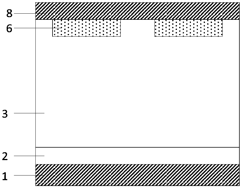
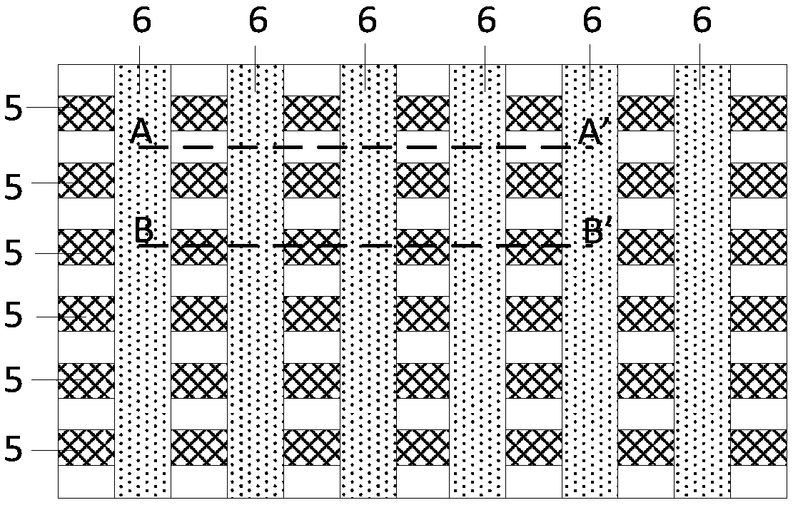
[0035] Embodiment 1: as figure 2As shown, a high withstand voltage silicon carbide Schottky diode is provided, including a semiconductor substrate, and the semiconductor substrate includes an N-type silicon carbide substrate 2 and an N-type silicon carbide epitaxial layer on the N-type silicon carbide substrate 2 3. In the cross-sectional direction of the device, a cathode metal 1, an N-type silicon carbide substrate 2, an N-type silicon carbide epitaxial layer 3, and an anode metal 8 are sequentially arranged from bottom to top, and in the N-type silicon carbide epitaxial layer 3 The upper part is provided with several strip-shaped first P-type well regions 6 separated at intervals and strip-shaped first N-type well regions 7 between adjacent strip-shaped first P-type well regions 6. The anode metal 8 and the The strip-shaped first N-type well region 7 is in Schottky contact, and the anode metal 8 is in ohmic contact with the strip-shaped first P-type well region 6; a cathod...


PUM


Abstract

The invention belongs to the technical field of manufacturing semiconductor devices, the invention relates to a silicon carbide Schottky diode with high withstand voltage, A semiconductor substrate comprises an N-type silicon carbide substrate and an N-type silicon carbide epitaxial layer, the upper part of the N-type silicon carbide epitaxial layer is provided with a plurality of spaced apart strip-shaped first P-type well regions and strip-shaped first N-type well regions, A plurality of stripe-shaped second P-type well regions and stripe-shaped second N-type well regions are arranged belowor on the lower surface of the stripe-shaped first P-type well region and the stripe-shaped first N-type well region respectively, and the stripe-shaped first P-type well region and the stripe-shapedsecond P-type well region are respectively at angles of 30 degrees to 90 degrees; A stripe-shaped second P-type well region with a certain angle with the stripe-shaped first P-type well region is arranged below the stripe-shaped first P-type well region, and the doping concentration of the stripe-shaped N-type well region in the stripe-shaped P-type well region is increased at the same time, the breakdown voltage of the device is greatly increased, and the surge current capability of the device is improved.

Description

technical field [0001] The invention relates to a diode and a manufacturing method, in particular to a high withstand voltage silicon carbide Schottky diode and a manufacturing method thereof, belonging to the technical field of manufacturing semiconductor devices. Background technique [0002] Power devices and their modules provide an effective way to realize the conversion of various forms of electric energy, and have been widely used in national defense construction, transportation, industrial production, medical and health and other fields. Since the first power device application in the 1950s, each generation of power devices has enabled more efficient conversion and use of energy. [0003] Traditional power devices and modules are dominated by silicon-based power devices, mainly thyristors, power diodes, power triodes, power MOSFETs and insulated gate field effect transistors, which have been widely used in the full power range. History, very mature design technology...

Claims


Application Information

Patent Timeline
Patent Type & Authority Applications(China)
IPC IPC(8): H01L29/872H01L29/06H01L21/04
CPCH01L29/872H01L29/0619H01L29/6606
Inventor 朱袁正周锦程杨卓叶鹏
Owner WUXI NCE POWER
Why Eureka
Try Eureka